
Official websites use .gov
A .gov website belongs to an official government organization in the United States.
Secure .gov websites use HTTPS
A lock (
) or https:// means you’ve safely connected to the .gov website. Share sensitive information only on official, secure websites.
Leveling-Up SEM Measurements for Chip Manufacturing
NIST and KLA Corporation develop electron-beam tilt measurement technique to help improve SEM quality
Researchers from the National Institute of Standards and Technology (NIST) and KLA Corporation, a provider of inspection and measurement systems for the semiconductor and related industries, have improved the accuracy of scanning electron microscope (SEM) measurements. Used for process control applications in semiconductor manufacturing, SEMs help ensure high-yield production of functional, high-performance chips.
A SEM uses a focused electron beam to image features as small as one nanometer, making it an important instrument for characterizing semiconductor device structures. During chip manufacturing, high-resolution SEMs are used for many inspection and metrology applications, including detection of very small defects, identification and classification of defects found by optical inspectors, critical dimension measurements of pattern features, overlay measurements, and more. This information helps chip engineers characterize and fine tune their manufacturing processes.
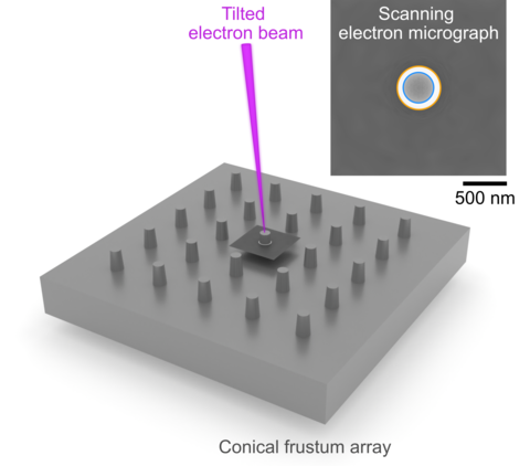
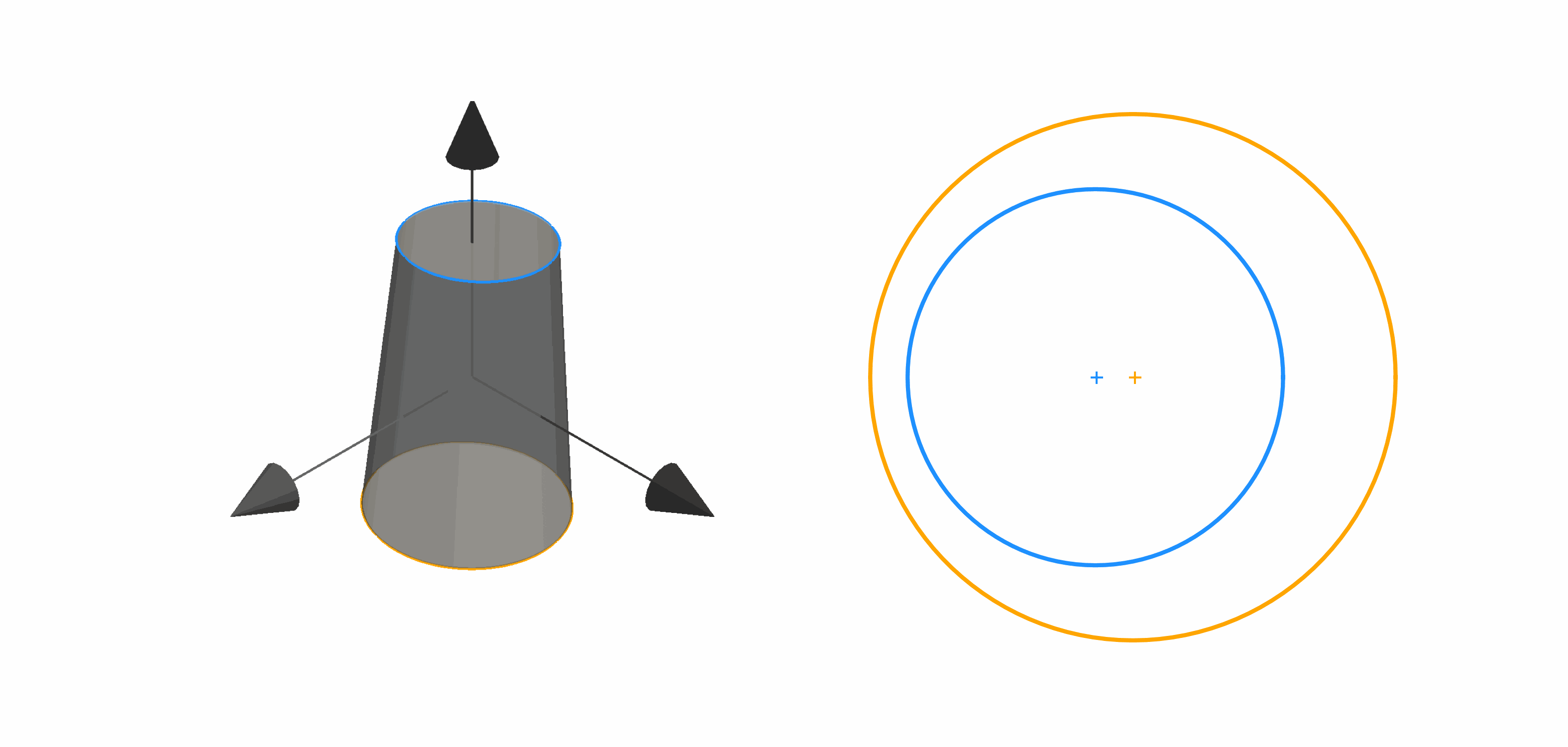
As the electron beam travels through a SEM, it is carefully controlled. A slight deviation of the electron beam from the ideal path or a tiny misalignment of the angle at which the beam strikes the surface of the chip can distort the resulting SEM image and misrepresent the structure of the device. NIST and KLA improved the accuracy of SEMs by accounting for these angular misalignments of the electron beam. The joint research project measures beam tilt with an accuracy of less than one milliradian, or five hundredths of a degree, which required advances in angular resolution and measurement validation.
To measure the beam tilt, NIST and KLA created a prototype standard for electron microscopy and analyzed the resulting electron micrographs in a new way. The prototype standard consists of an array of tapering pillars of silicon, known as conical frusta, which form images that are highly sensitive to beam tilt. The tilt shows up as a shift between the centers of images of the top and bottom edges of a frustum. Using their expertise in modeling electron–matter interactions, the researchers used simulations to demonstrate the potential for sub-milliradian accuracy, guiding their ongoing design and fabrication of the standard artifacts.
Arrays of conical frusta at known positions have the potential to measure any variation of the beam tilt across the region scanned and imaged by the SEM. Those measurements could further calibrate the magnification and distortion of the electron microscope. Furthermore, the new standard has applications to other microscopy methods used in chip manufacturing, including atomic-force and super-resolution optical microscopy. The ability to compare the results of different microscopy methods helps to reliably and reproducibly transfer information between the different methods and improve the accuracy of measurement models.
“Electron-beam tilt shifts the apparent positions of device features, reducing the accuracy of SEM measurements,” said Andrew C. Madison, NIST researcher and first author on industry papers covering this research. “Our new standard and analysis method can detect electron-beam shift as it varies across the imaging field.”
“With this data, SEM manufacturers can implement calibrations and corrections that improve image quality and measurement accuracy,” said NIST researcher and principal investigator Samuel M. Stavis.
“As experts in semiconductor inspection and metrology, we’re continually exploring new technologies that can extend current measurement limits,” said Yalin Xiong, senior vice president and general manager at KLA Corporation. “Collaboration with research organizations serves an important role in discovering innovations that can help advance process control for the chip industry. Our joint research with NIST is aimed at improving the accuracy of the fundamental measurements used to characterize chip manufacturing processes.”
NIST plans to make the new standard and analytical method broadly available to the chip manufacturing industry and the scientific community through publications and eventual distribution of frustum arrays.
Further details on the NIST-KLA joint development of methodologies and reference materials to enable precise and accurate measurement of electron-beam tilt will be presented during the International Conference on Electron, Ion and Photon Beam Technology and Nanofabrication (EIPBN), Session 4A on June 1, 2023, in San Francisco, California.
This project was performed under a Cooperative Research and Development Agreement (CRADA).
The identification of KLA Corporation is for information only and does not imply recommendation by NIST.
Reference:
A.C. Madison et al, Proc. SPIE 12496, Metrology, Inspection, and Process Control XXXVII, 1249606 (30 April 2023); https://www.spiedigitallibrary.org/conference-proceedings-of-spie/12496/1249606/A-total-shift-show--submilliradian-tilt-goniometry-in-scanning/10.1117/12.2673963.full