
Official websites use .gov
A .gov website belongs to an official government organization in the United States.
Secure .gov websites use HTTPS
A lock (
) or https:// means you’ve safely connected to the .gov website. Share sensitive information only on official, secure websites.
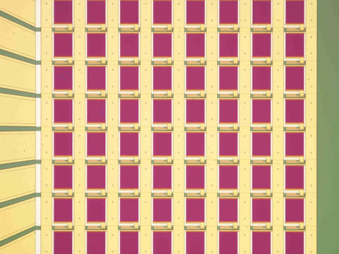
NIST Tile
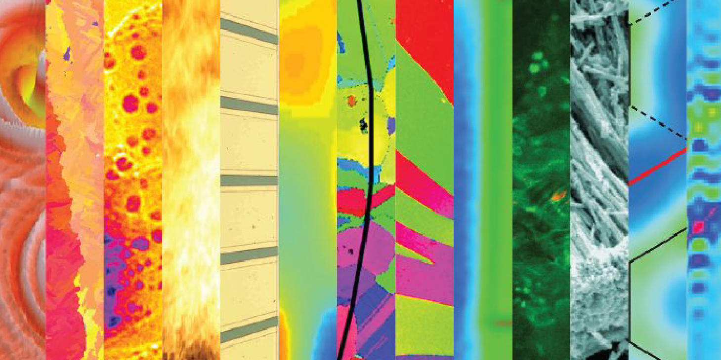
Curious about what each of the “strips” on this image represent? Read more below.
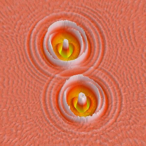
This simulation from 2005 shows how nanometer-scale devices can broadcast microwave signals that naturally synchronize and lock onto one another, similar to the way two fireflies would flash or two pendulum clocks would tick in sync.

Additive manufacturing — the process of melting down powder layer by layer into a 3D-printed design — can be stunning on the microscale.
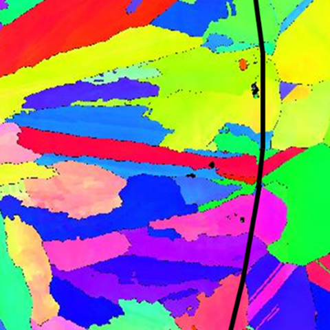
Each metallic grain’s orientation and crystalline structure in a 3D-printed design depends on the manufacturing process. Together, those structures can ultimately decide how the fully printed item responds to force (for example, how well a jet engine’s propeller resists centrifugal force while in motion). With a method called electron backscatter diffraction, NIST scientists plot out the structures in maps where each color pixel represents a grain’s orientation, which ultimately translates to its strength, flexibility, etc. By comparing the maps from one 3D-printing process to the next, manufacturers can decide which methods create results that best suit their needs.
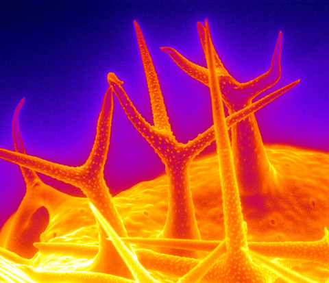
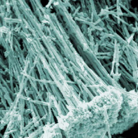
This colorized scanning electron microscope (SEM) image shows trichomes, which are hairlike structures on plants.
SEMs use electrons instead of light to illuminate their subjects. Because the wavelength of an electron can be up to 100,000 times shorter than that of visible light particles (photons), the electron microscope has higher resolution and can reveal much smaller structures. During the past 30 years, NIST researchers have performed a great deal of work to understand SEM instrument performance, instrument calibration, imaging and metrology. As technology improves, the need for standards grows. SEMs are routinely used as the primary tool to monitor semiconductor manufacturing processes. The field of view in this image is 0.37 millimeters.
False-color images, produced with neutron scattering, represent the nanoscale structures of single crystals of the piezoelectrics PZT. Piezoelectric materials are used in loudspeakers, sonar and other applications in which mechanical energy is converted to electricity or vice versa.
Because the atoms in high-performing PMN deviate slightly from their ideal positions, diffuse scattering results in a distinctive "butterfly" shape quite different from that of PZT, in which the atoms are more regularly spaced and performance is lower.
This research is helping to reveal why some of the best piezoelectric materials work as well as they do.
This micrograph shows a NIST sensor chip made of tungsten silicide. The chip’s 64 square detectors contain nanowires that convert a particle of light (photon) into an electrical pulse.
The sensor was used in a quantum Enigma machine — a quantum version of the famous World War II German encryption device. It was demonstrated at NIST in a collaborative experiment with the University of Rochester and Massachusetts Institute of Technology. NIST is a world leader in the development of single-photon detectors, used in applications ranging from quantum cryptography to astronomical telescopes.
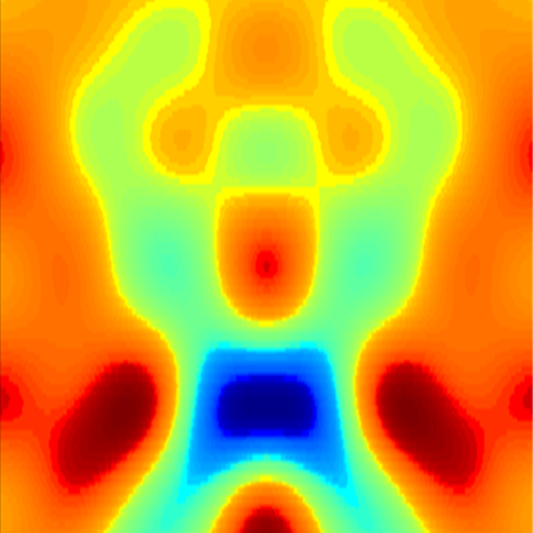
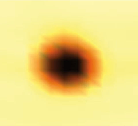
A strongman? Instead of seeing patterns in clouds, our scientists go to the microscope! NIST’s Ravi Attota uses a simple optical microscope and a technique called through-focus scanning optical microscopy to measure the dimensions of things at the nanoscale. Instead of trying to get one photo that’s clear and crisp, we take multiple blurry images, each at a different focus, to build a 3D view of the tiny objects. This particular image is of a silicon line on a silicon substrate.
From the minuscule trenches etched into microchips to a single nanoparticle resting on a silicon plate, scientists at NIST’s NanoFab facility as well as leaders in industry elsewhere send lots of items to Ravi and his team for measurement. The outcome might look out of this world, but the precision behind it is necessary for the technology and scientific advances all around us.
This image shows the microscopic structure of a piece of metal that was hit with a focused, high-power laser. It’s a way for us to study the crystal structure that forms as the melted metal resolidifies. The image comes from NIST’s work to develop benchmark tests for additive manufacturing, a way of creating products by layering a material based on a 3D model.

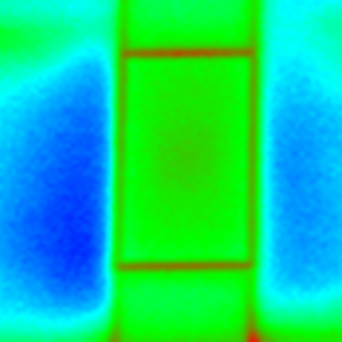
This image is of a glassy metal typically used in electrical transformers, which reduce voltages to household levels.
The image was made using scanning electron microscopy with polarization analysis (SEMPA), a technique that can see magnetic features as small as 10 nanometers. SEMPA reveals the underlying magnetic structure of a material by measuring the direction of its electrons’ spins, with different colors signifying the different directions of spin.
The larger bands of color represent desirable magnetic structures, while the “noise” in the upper right corner indicates defects that waste energy. Researchers made these measurements so that they could identify and find ways to reduce the sources of these defects.
The wall of two adjacent offices in 2008 — one modified to reduce energy flow and one as it was built in the 1960s — shown in infrared. In the modified room, scientists sealed all air leaks, added 9 inches of glass-fiber insulation to the exterior walls, replaced the 40-year-old single-pane glass window with a double-pane, argon-filled insulated glass window and installed a forced air heating and cooling unit. In this image, warm air escapes to the outside (orange and red colors) through the office with no modifications, while the other loses less heat.
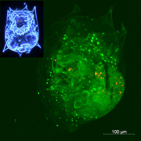
A close-up micrograph of an aquatic organism called rotifer Brachionus calyciflorus. In 2008, researchers fed the rotifer with a single-celled protozoan full of fluorescent quantum dots. You can see the quantum dots here in red, consumed as part of the rotifer's protozoan snack.
These metal oxide nanotubes formed thin films (about the width of a single human hair) that potentially could be used to measure the amount of gas emissions from a single cell, which could help us understand how cells communicate with one another and whether drugs or nanoparticles can harm them.
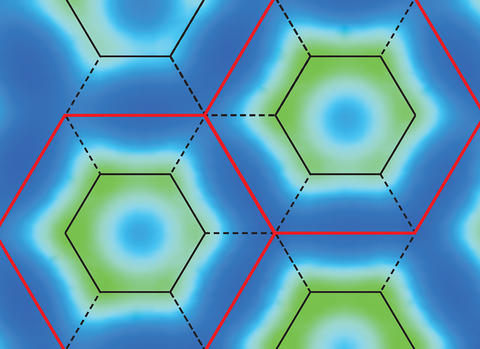
A “quantum spin liquid” is a theoretical new state of matter in which the electrons in magnetic atoms have spins that perpetually fluctuate, even at a temperature of absolute zero. Research into quantum spin liquids is important for understanding high-temperature superconductors and for developing quantum computers. This image, representing data from inelastic neutron scattering, represents the spin states in the quantum spin liquid candidate material Ca10Cr7O28.
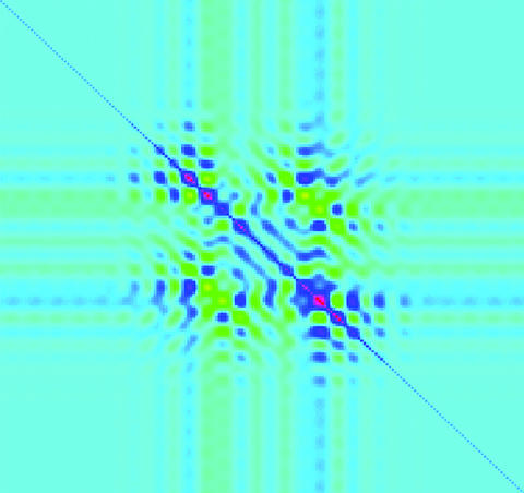
Images can help scientists visualize complex data. In this case, the patterns represent correlations among data taken while measuring a semiconductor device’s nanoscale features.
Today’s semiconductor industry depends on the performance of components that are just a few nanometers wide. Since the components are often too small to see using traditional microscopes, scientists need to get creative — in this case, by comparing experimental measurements with calculated values and seeing how well the values correlate.
Such NIST innovations directly impact the manufacturing of fast, mobile and energy-efficient electronics.