
Official websites use .gov
A .gov website belongs to an official government organization in the United States.
Secure .gov websites use HTTPS
A lock (
) or https:// means you’ve safely connected to the .gov website. Share sensitive information only on official, secure websites.
Thin-Film/Low-K Dielectric Constant Measurement
Thin-Film/Low-K Dielectric Constant Measurement
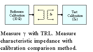
The methods developed in this project use measurements of both propagation constant and characteristic impedance to characterize planar transmission lines and determine the material properties of the thin films of which they are composed. This allows R, L, G, and C to be determined individually, and separates metal and dielectric loss. This is a joint project between the Electromagnetic Fields Group, Electromagnetic Properties of Materials Project and High Speed Electronics Project.
This project develops methods to accurately measure the electromagnetic properties of thin films from easy-to-perform in-situ transmission-line measurements. The project brings NIST's Electromagnetic Properties of Materials Group and the NIST MMIC Program into a collaborative effort with SEMATECH to develop
microstrip test vehicles, with Texas Instruments to develop coplanar waveguide test vehicles, and with DOW Chemical to investigate NIST fabricated test vehicles.
The methods are based on measurements of small printed transmission lines incorporating the materials to be characterized. They allow the dielectric constants of thin films and the conductivities of the metals used in the lines construction to be determined over broad frequency ranges.
The Coplanar Approach
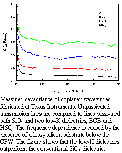
In a collaborative effort with Texas Instruments we designed experiments and fabricated and tested coplanar waveguides passivated with BCB, HSQ, and SiO2 films. The measurements convincingly demonstrate the approach.
The Microstrip Approach
Only a small portion of the electromagnetic energy in coplanar transmission lines is located in the passivation layer we would like to characterize. In a joint effort with SEMATECH we have designed microstrip test structures with greater sensitivity.
Testing for Materials Manufactures
We are using NIST's unique processing capabilities to pursue a very different approach to dielectric thin-film characterization at DOW Chemical, a major supplier of low-K dielectrics. In our collaboration with DOW we will perform most of the microfabrication at NIST; DOW will simply deposit and pattern the thin films on pretested circuits provided by NIST. A second set of measurements made at NIST will test for the differences in transmission-line capacitance.
References on: Planar Transmission Line Characterization and Electronic Materials Characterization