
Official websites use .gov
A .gov website belongs to an official government organization in the United States.
Secure .gov websites use HTTPS
A lock (
) or https:// means you’ve safely connected to the .gov website. Share sensitive information only on official, secure websites.
Thin Film Electronics (Archived)
Summary
The Thin Film Electronics Project develops rigorous measurements and methodology needed for continued U.S. leadership in manufacturing and innovation of emerging electronic devices.
Description
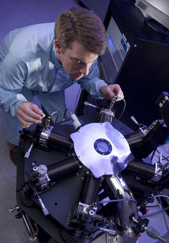
Figure 2. David Gundlach characterizes the electronic properties of single crystal organic field-effect transistors in a vacuum cryogenic probe station.
Today's electronics have reached a point where sheer computation power has yielded to combined form and function as the key driver of large consumer markets. The demand for portable and pervasive electronics with greater functionality promises significant changes over the next decades in how society interacts with each other and its surroundings. Such rapid and significant change requires continued improvements in traditional high performance low power electronics for informatics as well as entirely new device technologies based emerging electronic materials and novel integration methods to provide the specific functionality in the compliant form factor demanded. Examples of these new electronic materials and devices include: atomic, molecular, organic, atomic layer 2-D semiconductors, III-V, and metal oxide based transistors, optoelectronics, and sensors. As new concepts are being developed and demonstrated, a close coupling of technology and metrology development is also needed to continue to solidify our understanding and ensure a smooth transition to commercialization.
Therefore:
- We advance measurement science that precisely determines band alignment/offset at buried heterojunction interfaces and governs device operation in advanced ultra-low power high performance transistors.
- We develop novel methods and test structures to characterize the electromagnetic response of emerging atomic layer 2-D electronic materials over a broad spectral range for the design of advanced electronic/optoelectronic devices and which are critical to the stringent demands of process control in eventual manufacturing environments
- We create, combine, and correlate transient electronic and optoelectronic measurements for thin film electronic materials and devices to characterize their fundamental electronic processes and properties and provide the scientific foundation for innovation and diversity of new functional electronics
Major Accomplishments
2016
- Outstanding collaborative studies with IMEC and Starnet on advanced tunnel FET characterization
- Publication of high impact study on mobility overestimation in thin film transistors
- Ramp up to new infrastructure and measurements for novel thin film electronics (2D and flexible electronics, and advance batteries)
2015
- Developed transient contactless measurements to quantify charge density and recombination kinetics
- Initiated a new measurement science area in advanced battery research, based on intramural funding award.
2014
- Developed combined measurement methods to quantify charge density, lifetime, and recombination loss in next gen. solar cells
- Reported broadest spectral range measurements on the optical properties for the atomically thin semiconductor MoS2
2013
- Reported first definitive work on band alignment in heterojunction Tunnel FETs by using IPE
- Published seminal work on dirac point and Fermi level alignment at the graphene-insulator interface
Additional Technical Details
Technical Goals:
This objective is aligned with the project's general mission to establish measurements that quantify physical processes and electronic properties. These in turn open unforeseen pathways to manipulate such processes and properties for entirely new functionality and innovation in the electronics industry.