
Official websites use .gov
A .gov website belongs to an official government organization in the United States.
Secure .gov websites use HTTPS
A lock (
) or https:// means you’ve safely connected to the .gov website. Share sensitive information only on official, secure websites.
Summary
We develop new approaches to optical microscopy and electromagnetic modeling to enable improved metrology of nanoscale structures with dimensions more than an order of magnitude below traditional resolution limits. New applications and standards produced from these methods include defect inspection and critical dimension metrology for nanoelectronics.
Description
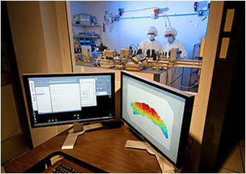
Figure 1. Clean-room conditions for the NIST 193 nm Microscope allow scientists to measure state-of-the-art nanoscale features.
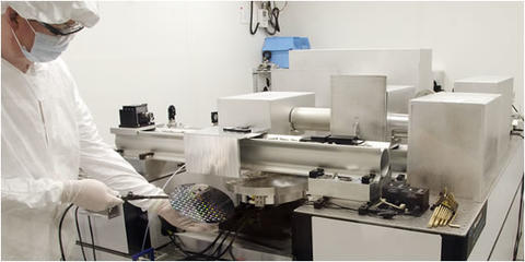
This project develops new approaches to optical microscopy based on a high magnification optical platform that samples the full 3-D scattered field. Both the semiconductor industry and the evolving nanomanufacturing sector are facing enormous challenges measuring nanometer scale features over large areas, needed for effective manufacturing process control of products that incorporate billions of nanoscale features. Optical microscopy is a high-throughput metrology methodology that provides a unique advantage since it is a high-bandwidth measurement method that is inherently parallel.
Measurements with sensitivity to features less than one-twentieth the wavelength can be made by analysis of scattered light profiles and the use of physics-based modeling. Extensive

electromagnetic modeling, developed in-house, enables quantitative metrology of nanoscale structures more than an order of magnitude below traditional resolution limits.
This project meets key NIST priorities in advanced manufacturing, energy, and photonics. We have had several contracts from the semiconductor industry as well as the Department of Energy for fuel-cell process control research. We have directly impacted semiconductor hardware platforms for optical overlay, defect, and critical dimension measurement. This project has also had a broad impact on the extensibility of optical methods for semiconductor manufacturing metrology. The project has launched a new effort to better describe the fundamental physics behind reductions in the optical constants of the next generation of nanoelectronic materials at reduced dimensions, such as nanowires. By providing quantitative values experimentally and from calculations, electromagnetic scattering can accurately meet future industry needs.
Major Accomplishments
2018
- Probed systematic errors caused by applying simplified two-dimensional (2-D) modeling to three-dimensional (3-D) arrayed nanostructures, which will become more apparent with decreasing lengths of these structures. Experimental setups, e.g., illumination numerical apertures and focal ranges, were proposed to increase the validity of the 2-D approach.
- Compared thickness-dependent optical scattering trends between hydrogen-terminated Si(100) and Si(111) by pairing density-functional theory (DFT) and our electromagnetic scattering codes. Developed new proficiencies in DFT, a computational quantum mechanical modelling method, which yields Kohn-Sham wavefunctions used to approximate the dielectric function for atomic-scale features
2017
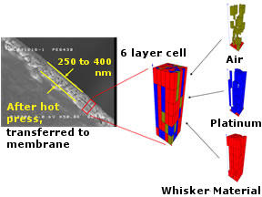
- First demonstration in the literature of visible-light optical reflection as a viable catalyst-loading monitor for the membrane exchange assembly (MEA) for proton exchange membrane fuel cells, with three separate optical methods qualitatively sensitive to Pt loading on MEA soft goods.
- Illustrating hidden errors in measuring dimensions when using electromagnetic modeling when size-dependent changes in the optical constants are neglected and also when 2D models are applied to ever-smaller 3D nanostructures.
- Surveying through simulation multiple illumination wavelengths from the deep ultra-violet down to the extreme-ultraviolet to quantify direct improvements to defect detectability using wavelengths as short as 47 nm.
2016
- 2016 Department of Commerce Silver Medal to Bryan Barnes and Rick Silver “For pioneering advances in optics, imaging structures 30 times smaller than the wavelength of light with near atomic accuracy.”
- Demonstrating to the semiconductor industry finite arrays of lines with areas much smaller than the microscope's field-of view, a key step towards more accurate measurement of critical dimensions such as the line width.
2015
- Completing first major upgrade to the NIST λ = 193 nm microscope enabling 10x fluence, illumination and collection path filtering, and future interferometric solutions.
- Addressed the effects of line edge and line width roughness (LER, LWR) upon both defect measurements (e.g., false positives) and also optical parametric measurements of line width and height (e.g., systematic biases).
2014
- Hybridized sub-20 nm wide arrays of lines from both Intel and from SEMATECH.
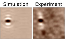
- Detected defects with widths as small as (16 ± 2) nm, or 1/12th the wavelength, without modeling using a new 3-D volumetric approach that uses all the scattered intensity data in xyz space.
2013
- 2013 R&D 100 Award for "Quantitative Hybrid Metrology," a new method that enhances multiple measuring instruments by tying them together statistically in novel combinations. Hybrid adopted publically by IBM, GlobalFoundries, Nova, and others.
- 2013 Intel Outstanding Researcher in Metrology Award, noting "This work is both fundamentally unique and technically important to the industry... scatterfield microscopy helped spur industry wide interest."