Summary
This program aims to develop the metrology to enable quantitative assessment of performance limiting reliability issues, and to describe the physics of failure related to new materials, processes, and integration schemes for emerging integrated systems that could allow extremely high energy efficient information processing. The new functionality requirements of emerging information processing paradigms drive the development of novel devices, which in turn requires new materials and integration schemes (e.g., high mobility materials in three-dimensional integrated systems (3D-IC)). The scope of the program includes, but not limited to atomistic understanding of the intrinsic properties of emerging materials and their applications in the interconnect of advanced electronics (e.g., 3-D, heterogenous- and printed electronics). The metrology tools and techniques that we are developing leverage broadband dielectric spectroscopic evaluation of accelerated thermo-mechanical and other stress aging of materials and integrated systems.
Description

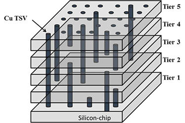
Schematic diagram of a 3D stacked integrated circuit (3D-SIC), achieved using copper through-silicon via (TSV) interconnects.
The Emerging Integrated Systems Metrology program supports measurements for advanced manufacturing and secure nano-manufacturing, novel devices and electronic materials. Specifically, the program aims to develop the metrology required to enable a quantitative assessment and physical understanding of performance limiting reliability issues in emerging electronic devices from the perspectives of new materials, processes, and integration schemes to enable physics of failure (PoF) approaches to reliability assessments. The ultimate sizes and functionality of the emerging devices will be defined by the fundamental and engineering limits such as heat dissipation, carrier mobility and fault tolerance thresholds. At present, it is unclear which are the best measurement methods needed to evaluate the nanometer-scale features of such devices and how the fundamental limits will affect the required metrology. The metrology being developed in this program will allow new functionalities to support emerging information processing paradigms drive the development of novel devices, which in turn requires new materials and integration schemes (e.g., high mobility materials in three-dimensional integrated systems (3D-IC)). The ultimate output of this program will be as an enabling support for “designed for reliability” approaches in nano-manufacturing of advanced integrated systems. We collaborate extensively with both internal and external entities, such as semiconductor industry consortia, universities and other research institutions to use direct experimental measurements and inferred root causes of failure to inform modeling and simulation analyses, to address various reliability and failure mechanisms in electronic devices.

The projects within this program include the characterization and understanding of the entire interconnect system (i.e., the wiring and the associated insulating dielectric layers) and packaging of such electronic devices. The developed metrology and documentary standards we develop will aid advanced manufacturing, heterogeneous integration, security and commercialization of advanced complex integrated systems. Towards this end, the following are some of the current projects within the program:
- New Material Characterization
- Detection and characterizing of electrically active defects (e.g., dangling bonds in dielectrics in integrated devices),
- Non-contact electrical measurements of inherent properties of high mobility (e.g., III-V, low dimensional, phase change, etc.) materials,
- Spectroscopic (UV-Visible-NIR) measurements of inherent properties of high mobility (e.g., III-V, low dimensional, phase change, etc.) materials,
- Use of microwave/ radio frequency (RF) based dielectric spectroscopic methods for assessment of material property changes in advanced interconnect systems (i.e., dielectric and metallic material aging, such as copper TSVs,
- Use of synchrotron-based X-ray micro-beam sources for depth-dependent measurement of the full stress tensors in interconnects used for 3-D integrated circuits (3-D ICs).
- Interconnect Reliability
- Contact formation (i.e., atomistic interaction between metal and emerging dielectrics)
- Localized modification of material properties in nanoscale devices, to generate unique identification signatures.
- Non-destructive electrical metrology for detection of defects and metal interconnects in the nanoscale regime.
- Thermo-mechanical reliability of integrated systems (i.e., microwave characterization of dense I/O boards, electromigration in TSV-enabled 3D-ICs, etc.)
- Simulation and modeling of electromagnetic and RF measurements using finite element methods.
Major Accomplishments

- Working with leading semiconductor industry consortia, we demonstrated RF detection of incipient joint defects in high density I/O boards.
- Demonstrated RF detection and monitoring of passivation failure and subsequent interconnect corrosion of 3D-TSV enabled ICs.
2018
- Demonstrated RF detection and monitoring of pre electromigration failure in 3D-TSV enabled ICs.
- Demonstrated the reliability impact of Cu interconnect texture engineering through electroplating process control
2017
- Demonstrated the feasibility of using broadband RF monitoring to understand the elementary events that occur in the early stages of electromigration in integrated 3D systems.
- Used broadband RF monitoring of atomistic changes in materials to demonstrate an understanding of early failures behavior during integrated devices burn-in.

