
Official websites use .gov
A .gov website belongs to an official government organization in the United States.
Secure .gov websites use HTTPS
A lock (
) or https:// means you’ve safely connected to the .gov website. Share sensitive information only on official, secure websites.
Summary
Precise measurements of thermal properties at the nanoscale are needed to engineer advanced and heterogeneously integrated devices, but measurements at this scale are currently unattainable. This project will radically advance thermal metrology by developing new tools for mapping thermal conductivity and interfacial thermal conductance at the nanoscale, with high precision and throughput. These advancements have significant implications for semiconductor stakeholders in government, academia, and industry.
This project will better position the U.S. semiconductor industry for measuring new and nanoscale materials.
Grand Challenge 2. Advanced Metrology for Future Microelectronics Manufacturing
Description
Continuous advances in the performance and functionality of semiconductor devices have been driven by scale reduction, incorporation of new and nanomaterials, and by heterogeneous integration (HI). However, such scaling and integrated architecture has rendered existing thermal metrology inadequate to meet current and future needs.
New measurements are critically needed to validate modelling and engineer advanced devices based on existing, new, and nano materials.
By developing two new tools for measuring thermal properties of materials, interfaces, and devices at the nanoscale, with high precision and throughput this project will satisfy several unmet needs within the semiconductor ecosystem.
These advances in metrology will facilitate the co-design and integration of advanced packaging solutions and shorten the development cycle of advanced semiconductor devices by providing reliable data for simulations of devices and chiplets. Furthermore, the ultrahigh throughput, super resolution microscope could be commercialized aiding both development and quality control for U.S. semiconductor infrastructure.
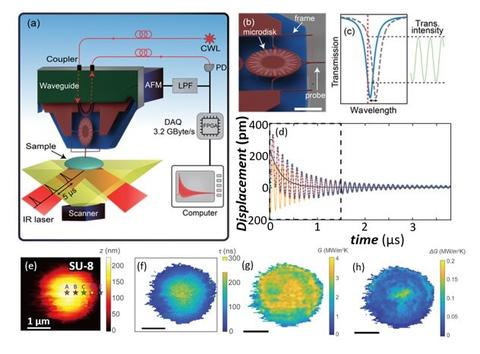
(a) Schematic of existing (bottom illumination) NIST PTIR setup using a silicon optomechanical AFM probe. (b) False-colored scanning electron micrograph of the transducer. The scale bar is 5 µm. c) Schematic depicting one of the transducer’s whispering gallery optical resonances (blue) and the CWL working wavelength (dashed red line). (d) Measured PTIR signal (e) AFM topography of a SU-8 sample and simultaneously recorded maps of the sample thermalization time (τ) (f), G (g) and ΔG (h).