
Official websites use .gov
A .gov website belongs to an official government organization in the United States.
Secure .gov websites use HTTPS
A lock (
) or https:// means you’ve safely connected to the .gov website. Share sensitive information only on official, secure websites.
Summary
The information economy – the modern economy that heavily dependent on information gathering, transmitting, processing, storing, utilizing and consuming is built upon nanoscale electron devices. With electron devices reaching the limit of physical laws, it is very difficult to measure the various parameters that provide the understanding needed to overcome the limitations. In addition, new devices based on new materials are increasingly part of the whole electronics systems and these new devices need new measurement methods. Systems built with these devices must function reliability over the intended service time. As the number of electron devices in a system reach beyond a trillion, the probability of failure also increases. Many electronic systems such as air traffic control, automobile, airplane, medical equipment, etc. cannot afford to fail because lives are at stake. The fundamental measurement challenge is: how to ensure the life of a system from the measurements of its basic building block - individual devices? This project examines many measurement methods critically as well as develop new measurements to meet this challenge.
Description
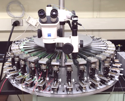
Massively parallel wafer-level long-term reliability test system featuring 30 fully functioning mini probe stations each supporting 100 probe pins with all the supporting stress/measure electronics integrated (without cables). Each mini probe station supports up to 600ºC.
Over the decades, many measurement methods were developed to meet the needs of advancing electron device/circuit/system technology. As technology continue to advance, new needs continue to surface, either due to old measurements are no longer adequate or due to no established method exists. A case in point is the need to measure the series resistance of a high-performance transistor. All existing measurement methods have known deficiencies, and better method is urgently needed because series resistance is dominating the performance of the transistor. To meet that challenge, we developed a novel series resistance extraction method that uses a single device instead of the common device array method which necessitate the use of assumption that is known to be not true.
As electron devices get smaller, our ability to understand what is going on inside becomes more limited. As proper measurements are essential for gaining better understanding, the development of novel new measurements is more important than ever. Furthermore, the line between meeting the need of technology and the need of fundamental physics blurs. For example, device heat generation, heat transfer and distribution are critical aspect of performance and reliability. Some devices depend on highly confined heating to function (Phase-change memory, for example) and some must control the un-wanted but unavoidable heating (self-heating effect on advanced MOSFET). Measuring the temperature in nanoscale devices is a challenge that remains to be met. How do you measure temperature when temperature itself has no meaning? (temperature is a statistical quantity that becomes invalid at dimension smaller than the phonon mean-free-path).
Electron devices are not perfect and defect sites can trap charges. Sometimes, that is leveraged to become a feature (non-volatile memory) and most of the time it is a reliability problem. How to detect these defects and identify what they are so that ways to eliminated them can be found. As electron devices becomes smaller, even a single trapped charge can destroy the device characteristics and put an entire system at risk. This requires extraordinary sensitive method to detect and identify the defects. We demonstrated single defect detection even when in the complication of gate leakage current by pushing the charge-pumping method to new height. However, able to detect a single defect does not mean we can identify the defect’s chemical nature or its structural nature. To that end, we are working on electrically-detected-magnetic-resonance (EDMR) spectroscopy which can potentially achieve that goal.
Reliability of electronic system is critically important in many ways. A jet liner’s electronic system failure can kill hundreds of people. An air traffic control system failure can shut down all air traffic for a period, greatly impacts the economy. The commerce department statistic shows that 90% of the business go into bankruptcy within a year after a data server failure lasting for a week or more. Survey shows that the top priority of all data center hardware purchase is reliability. With such importance, why failure still occurs? The answer lies in the scale of modern electronics system. Even as simple as a smart phone, there are tens of billions of transistors working together and even one transistor failure can lead to system failure. Statistic says such system will never work. However, we know that smart phone and even larger systems work. The magic is in redundancy and design-in margin. It all come with costs. The bigger the system, the more costly it is to provide such reliability coverage. When system get too large, such as exascale computers, all the tricks in the world will not make it work without improving the reliability of the fundamental building block – the individual electron device. Thus, we view device reliability as the most critical aspect of the fourth industrial revolution that is data centric.
Reliability, or device degradation is fundamentally a statistical phenomenon. Defects are created in the device during manufacturing or during field use randomly. Thus, to assure that systems made with trillions of devices can function reliably for the intended period (20 years for automobile, for example), measurement must be done in a statistically sound manner. Therein lies the biggest challenge in reliability measurement. Large number of devices must be measured for a very long time just to investigate one mode of failure, and there are many modes of failure. To make a step in the right direction, we developed a massively parallel wafer-level long-term reliability test system, increasing the devices under test in a probe station by nearly one thousand-fold.
The first application of such a test system was on the breakdown reliability of gate oxide in SIC power MOSFET. We demonstrated how important is sample size (number of devices under test) in capturing the failure mode and based on that developed a new “luck defect” model to help guide manufacturers to solve the problem.
It is the development of reliable physics model based on data collect from properly design measurement that allow the long-term reliability of a system to be projected. Our goal is to critically examine various degradation modes and develop physics model for life-time projection with high confident level. With such models, redundancy and reliability margin can be better managed to achieve reliability at an affordable cost.