
Official websites use .gov
A .gov website belongs to an official government organization in the United States.
Secure .gov websites use HTTPS
A lock (
) or https:// means you’ve safely connected to the .gov website. Share sensitive information only on official, secure websites.
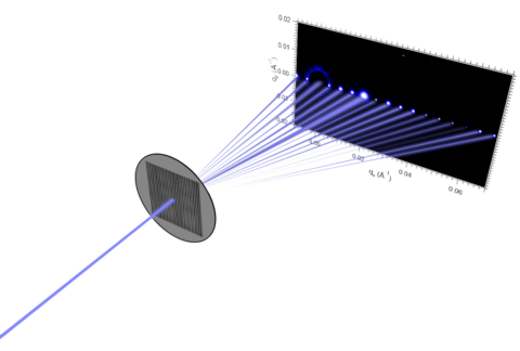
Critical Dimension Small Angle X-Ray Scattering (CDSAXS) for Next Generation in-line Metrology
Summary
The semiconductor industry is in need of new, high throughput in-line dimensional metrology methods to characterize next generation 3D nanostructures. The industry currently uses optical scatterometry for process control to monitor feature size and shape. As devices get smaller and more 3D, optical scatterometry is reaching fundamental limits. NIST has developed a method called Critical Dimension Small Angle X-ray Scattering (CDSAXS) for next generation dimensional metrology.
This project will expand the development effort at NIST for critical dimension small angle X-ray scattering (CDSAXS) to address critical industry needs for in-line dimensional metrology.
Grand Challenge 2. Advanced Metrology for Future Microelectronics Manufacturing
Description
The semiconductor industry is in need of new in-line dimensional metrology methods to measure the size and shape of nanoscale structures such as gate-all-around transistors, 3D-NAND, and 3D-DRAM for process control. The NIST-developed CDSAXS method has recently been commercialized for characterization of 3D-NAND contact holes and has the potential to provide need measurements of gate-all-around (GAA) nanosheet transistor and through silicon vias (TSV).
The industry needs NIST to use their unique expertise in the CDSAXS method to provide continued support through advanced measurement and standard development. NIST will leverage our strong connections with the semiconductor industry to identify the most pressing needs in CDSAXS and to transfer developed technology so that it can be applied to the fabs as soon as possible.
You can’t make what you can’t see. The shape and size of nanoscale devices determines their properties. Reliable manufacturing with high yield requires metrology feedback.
The project will continue the development and application of a NIST-invented next generation dimensional metrology method to provide needed measurements of advanced 3D nanoscale structures. The project will allow NIST to provide needed support through advanced measurement development and creation of relevant standard reference materials to enable metrology companies to provide the measurement solutions that fabs need.
There is an urgent need now by the industry for better dimensional metrology and for IP-neutral test structures. For longer term application of CDSAXS, NIST will closely work with companies developing new X-ray sources to identify if they will work for CDSAXS and if they do, help them to demonstrate and accelerate their adoption by metrology companies into fab-ready tools.
Demonstration of CDSAXS measurements on advanced device structures and using novel X-ray sources will provide a path towards the needed improvements in metrology tools. The IP-neutral test structures will provide a common platform for metrology vendors to develop and test their next generation instrumentation and methods.