

Official websites use .gov
A .gov website belongs to an official government organization in the United States.

Secure .gov websites use HTTPS
A lock (
) or https:// means you’ve safely connected to the .gov website. Share sensitive information only on official, secure websites.


High-Frequency Electronics
Summary
The High-Frequency Electronics project supports advanced communications, millimeter-wave technologies, and the semiconductor industry through research of high-frequency on-wafer metrology and the development of electronics-based metrology instrumentation. This work spans the application of accurate measurement techniques and characterization methods to on-wafer and over-the-air (OTA) components; design and characterization of high-frequency circuits realized using cutting-edge technologies; and extending the application of accurate electronic instrumentation to ever more complicated applications. Ultimately, the work in this project facilitates the adoption of new technology by industry by providing accurate assessments and improved techniques and models to be used in design and integration.
With our small-signal measurement capability already reaching 1.1 THz, our new sub-THz (100–300 GHz) large-signal measurement facility for on-wafer testing of semiconductor transistors and active circuits provides semiconductor foundries with essential measurement data to develop advanced technologies, optimize fabrication processes, and enable next-generation millimeter-wave and sub-THz applications.
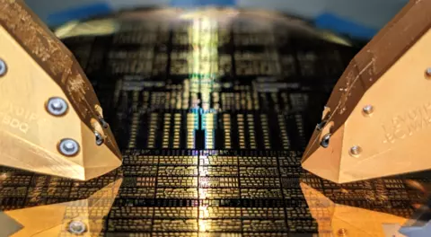
Description
This project addresses the hardware and calibration challenges of mm-Wave and THz device measurements in the new communication bands beyond 5G architectures and other emerging applications above 100 GHz. We develop new calibration and measurement approaches to support the entire development cycle for high-frequency architectures, including transistor measurement, modeling and design techniques, model verification, on-wafer circuit test at both component and system-performance levels, quantitative OTA system-level test and the development of novel high-precision instruments and sources above 100 GHz.
This project addresses research gaps in the 7 technical areas:
- Develop advanced on-wafer calibration standards in semiconductor foundry process and new calibration procedures
- Develop characterization techniques for millimeter-wave/ sub-THz transistors and microelectronic circuits
- Develop reliable transistor models that include manufacturing variation for circuit simulators
- Fabrication and realization of integrated active circuits with nominal expected designed RF performance (i.e. 1st pass design success)
- Investigate new approaches to on-wafer RF reference sources using electronics and phototransistors to develop advanced instrumentation
- Metrology for on-wafer to over-the-air measurements and characterizations
- Applying machine learning techniques to improve the state-of-the-art advanced calibration and circuit design
This project currently supports semiconductor foundries through Cooperative Research and Development Agreements (CRADAs) and government programs (DARPA ELGAR and CHIPS metrology program). Our university collaborations are established through Measurement Science and Engineering (MSE) research grants and the Professional Research Experience Program (PREP).
Activities
Development of advanced on-wafer calibration standards in semiconductor processes. The goal is to develop new on-wafer calibration structures and advanced calibration procedures up to THz frequencies, with the objective to reduce measurement errors. We first design custom shielded calibration standards directly in semiconductor foundry processes to suppress substrate modes and investigate new calibration procedures to mitigate and account for undesired propagation paths such as probe-to-probe coupling. The best practices in the design of on-wafer standards and calibration procedures are reported in [1], with validation up to 1.1 THz. The on-chip calibration techniques can be applied to monolithic, hybrid, and 3D heterogeneously integrated circuits.
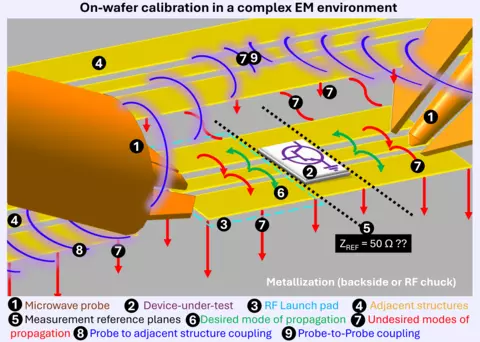
Advanced measurement techniques for high-frequency microelectronic applications. Adopting advanced calibration procedures, we develop unique large signal load-pull characterization in the millimeter-wave and sub-THz frequency ranges to accurately measure transistor and circuit RF performance. In 2026, we successfully validated new large-signal measurement setups with reduced measurement errors at 220 GHz. We measured and reported state-of-the-art load-pull performance [see list of publications] of InP, GaN, SiGe transistors from various US semiconductor foundries. We are working to develop higher-power and noise measurement capabilities above 100 GHz, as well as non-linear characterization with absolute phase calibrations.
High-frequency compact transistor models. The work of this project in developing more accurate transistor models is essential to the design of high-frequency circuits at low cost with expected performance. Transistor models, used in circuit simulators to design various integrated circuits, fail to accurately predict the actual performance of the transistor at millimeter wave frequencies and beyond. Several circuit fabrication cycles are consequently required to achieve expected RF performance. To accelerate innovation and reduce fabrication cost, we develop more reliable transistor compact models using advanced calibration and measurement techniques developed under this project. A key goal consists of integrating transistor manufacturing variation in transistor compact models to predict yield prior fabrication.
Integrated-circuit designs in semiconductor processes. We design innovative integrated structures and circuits up to 1 THz to support metrology across various NIST projects. We thoroughly take advantage of semiconductor processes that offer innovative design solutions for on-chip standards, transistor test structures, high power amplifiers for instrumentation, on-wafer sources based on oscillators and phototransistors, multipliers, mixers, and pulse generators that are designed and fabricated in US semiconductor foundry processes. Additionally, including process variation in the circuit design and optimization process will allow the determination of optimal design parameters under this variation, allowing users to assess the efficacy of a realized design, and facilitate improved designs and increased yields. This requires advanced optimization algorithms that are being developed in collaboration with university partners.
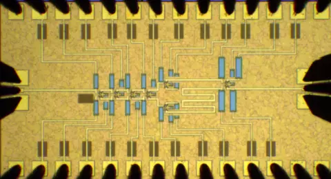
Sub-THz frequency sources referenced to optical sources Sub-THz electronics require on-wafer chip-scale sources with low phase noise and high frequency resolution. These high-fidelity sources can be achieved by driving photo mixers, photo diodes, and photo-sensitive transistors with optical beat notes generated from laser combs or dual-laser sources. Such opto-electronic sources already find practical applications up to THz frequencies. We develop new Sub-THz devices such as photo-mixers, phototransistors, and novel optically-injection locked oscillators, as well as compact models to efficiently connect optoelectronic devices to solid-state electronics in integrated THz systems.
Over-the-Air measurements and traceability: As the communications industry moves to more compact and embedded circuitry, connectorized RF test ports are often unavailable. Nevertheless, industry demands testing methodologies which must now be performed over-the-air. This project supports these efforts by extending our calibration expertise to produce traceable over-the-air measurements. This work enables the accurate characterization of next generation wireless communications systems.
Electronics for G-band Arrays (DARPA): We are applying our measurement, calibration and characterization expertise to help evaluate the performance of next generation G-band (170 to 260 GHz) circuits designed for communication. This includes transistors and power amplifiers in bleeding-edge III-V technologies. As part of our partnership with commercial foundries, we provide guidance on calibration methodologies and design techniques and characterize performers’ devices and circuits. Additionally, we are an independent evaluator of fabricated circuits for this program. Through this work we are directly improving industry’s understanding of their own fabrication technology.
CHIPS metrology program: Metrology for High Frequency transistor models Advanced semiconductor technology has led to continuous performance improvements in transistors. However, many iterations are needed to obtain optimal performance, and the yield and reproducibility is incredibly poor. Furthermore, US chip manufacturers are ill-equipped with legacy measurement techniques and underperforming models. We propose a robust path to develop and verify high-frequency transistor models: 1) new on-wafer standards and calibration, 2) precision noise measurements for transistor quality assurance, 3) improved characterizations, 4) optimal models tailored to a given technology, and 5) transistor model verification across frequency with key performance indicators.
Current Measurement Capabilities
- On-wafer and waveguide Scattering parameters to 1.1 THz
- Large signal load-pull capability from 110 GHz to 170 GHz: high-power (20-30 dBm)
- Large signal load-pull capability from 170 GHz to 260 GHz: high-power (10-15 dBm)
- Multi-harmonic load-pull to 40 GHz
- Pulse IV system
- Electro-optic sampling
Major Accomplishments
- Sub-THz (100–300 GHz) large-signal load-pull measurement capability for on-wafer transistor testing, pairing cutting-edge instrumentation with advanced on-wafer calibrations. Record performance of 46% Power Added Efficiency reported at 125 GHz
- Advanced on-wafer mTRL calibration kits demonstrated in various semiconductor processes (InP, SiGe, GaN) from 100 MHz to 1.1 THz
- Developed innovative microelectronic integrated circuits for new instrumentation, including on-wafer phase reference above 110 GHz and broadband THz amplifiers in InP HBT processes
- Best paper award: 2021 IEEE BiCMOS and Compound Semiconductor Integrated Circuits and Technology Symposium (BCICTS) “High-Gain 500-GHz InP HBT Power Amplifiers”
Additional Technical Details
List of publications from High-Frequency-Electronics project (past 5 years)
[1] J. Cheron et al. “Terahertz On-Wafer Microelectronic Characterization in Various Semiconductor Processes” accepted in Microwave Magazine 2026
[2] J. Molles et al. “D-band GaN HEMT Load-Pull Performance Comparing TRL and mTRL Calibrations” accepted in EUMW 2026
[3] J. Cheron et al. “InP HEMT Load-Pull Performance Demonstrating 46% Power-Added-Efficiency at D-Band Frequencies” accepted in BCICTS 2026
[4] R. D. Jones et al., "Accurate Load–Pull on InP HBT and InP HEMT Devices, Achieving Above 30% PAE at 220 GHz," in IEEE Microwave and Wireless Technology Letters, doi: 10.1109/LMWT.2026.3677605.
[5] J. A. Jargon, D. Gu, J. Cheron, R. D. Jones and A. A. Koepke, "Quantifying Variance Components for Repeated Scattering-Parameter Measurements up to 110 GHz," 2026 106th ARFTG Microwave Measurement Conference (ARFTG), Los Angeles, CA, USA, 2026, pp. 1-4, doi: 10.1109/ARFTG68976.2026.11475008.
[6] T. Bonnen et al., "A Comparison of On-Wafer Microstrip and Grounded Coplanar Waveguide Multiline-TRL Calibration for Millimeter-Wave GaN HEMT Characterization," 2026 106th ARFTG Microwave Measurement Conference (ARFTG), Los Angeles, CA, USA, 2026, pp. 1-4, doi: 10.1109/ARFTG68976.2026.11475018.
[7] J. Cheron, R. D. Jones, C. Evanovich, J. A. Jargon, B. F. Jamroz and P. H. Aaen, "Evaluating Probe-to-Probe Crosstalk Prior to on-Wafer Transistor Characterization," 2025 IEEE BiCMOS and Compound Semiconductor Integrated Circuits and Technology Symposium (BCICTS), Phoenix, AZ, USA, 2025, pp. 1-4, doi: 10.1109/BCICTS63111.2025.11211372.
[8] P. Blomberg, J. Cheron, H. Rodilla and J. Stake, "Effects of ground-to-ground connections on coplanar waveguide calibration standards for terahertz on-wafer measurements," 2025 50th International Conference on Infrared, Millimeter, and Terahertz Waves (IRMMW-THz), Helsinki, Finland, 2025, pp. 1-2, doi: 10.1109/IRMMW-THz61557.2025.11320108.
[9] J. Cheron et al., "Improving On-Wafer Characterization of Sub-THz Devices: A Probe Influence and Crosstalk Study," in IEEE Transactions on Microwave Theory and Techniques, vol. 73, no. 6, pp. 3144-3155, June 2025, doi: 10.1109/TMTT.2025.3550095.
[10] J. Shell, J. Cheron, M. Hodek, E. Gebara and N. C. Miller, "Impact of Uncertainty and Non-Idealities in On-Wafer Multiline TRL Calibration on Broadband GaN HEMT Modeling," 2025 104th ARFTG Microwave Measurement Conference (ARFTG), San Juan, PR, USA, 2025, pp. 1-4, doi: 10.1109/ARFTG63706.2025.10989797.
[11] R. D. Jones et al., "A Technique for Optimal On-Wafer Device Spacing at Millimeter-Wave Frequencies," in IEEE Microwave and Wireless Technology Letters, vol. 35, no. 3, pp. 370-373, March 2025, doi: 10.1109/LMWT.2024.3522810.
[12] R. D. Jones, J. Cheron, B. F. Jamroz, A. D. Feldman and P. H. Aaen, "Small-Signal Model Verification and Analysis of Unmatched Multi-Finger HBT Cells at 220 GHz," 2024 IEEE BiCMOS and Compound Semiconductor Integrated Circuits and Technology Symposium (BCICTS), Fort Lauderdale, FL, USA, 2024, pp. 76-79, doi: 10.1109/BCICTS59662.2024.10745687.
[13] J. Cheron, R. D. Jones, B. T. Bosworth, J. A. Jargon, B. F. Jamroz and A. D. Feldman, "Terahertz On-wafer mTRL Calibration Kits For Microelectronics Characterization," 2024 49th International Conference on Infrared, Millimeter, and Terahertz Waves (IRMMW-THz), Perth, Australia, 2024, pp. 1-2, doi: 10.1109/IRMMW-THz60956.2024.10697705.
[14] R. D. Jones et al., "On-Wafer Capacitor Characterization Including Uncertainty Estimates Up to 1.0 THz," in IEEE Transactions on Terahertz Science and Technology, vol. 14, no. 5, pp. 734-744, Sept. 2024, doi: 10.1109/TTHZ.2024.3431190.
[15] J. Cheron et al., "A 0.1 GHz to 1.1 THz Inverted Grounded-CPW mTRL Calibration Kit Characterization in an InP HBT Process," 2024 IEEE Wireless and Microwave Technology Conference (WAMICON), Clearwater, FL, USA, 2024, pp. 1-4, doi: 10.1109/WAMICON60123.2024.10522868.
[16] R. D. Jones et al., "Microstrip and Grounded CPW Calibration Kit Comparison for On-Wafer Transistor Characterization from 220 GHz to 325 GHz," 2023 IEEE BiCMOS and Compound Semiconductor Integrated Circuits and Technology Symposium (BCICTS), Monterey, CA, USA, 2023, pp. 124-127, doi: 10.1109/BCICTS54660.2023.10310853.
[17] J. Cheron, R. D. Jones, D. F. Williams and P. H. Aaen, "A Tunable 220 GHz Comb Generator Realized With an Ultrawideband Mixer in an InP HBT Technology," in IEEE Microwave and Wireless Technology Letters, vol. 33, no. 9, pp. 1345-1348, Sept. 2023, doi: 10.1109/LMWT.2023.3294299.
[18] J. Cheron et al., "A 110 GHz Comb Generator in a 250 nm InP HBT Technology," in IEEE Microwave and Wireless Components Letters, vol. 32, no. 6, pp. 736-739, June 2022, doi: 10.1109/LMWC.2022.3164511.
[19] J. Cheron et al., "Collector Series-Resistor to Stabilize a Broadband 400 GHz Common-Base Amplifier," in IEEE Transactions on Terahertz Science and Technology, vol. 12, no. 1, pp. 63-69, Jan. 2022, doi: 10.1109/TTHZ.2021.3119999.
[20] J. Cheron et al., "High-Gain 500-GHz InP HBT Power Amplifiers," 2021 IEEE BiCMOS and Compound Semiconductor Integrated Circuits and Technology Symposium (BCICTS), Monterey, CA, USA, 2021, pp. 1-4, doi: 10.1109/BCICTS50416.2021.9682464.