
Official websites use .gov
A .gov website belongs to an official government organization in the United States.
Secure .gov websites use HTTPS
A lock (
) or https:// means you’ve safely connected to the .gov website. Share sensitive information only on official, secure websites.
NanoFab Tool: Specialty Coating Systems PDS 2010 Parylene Deposition System
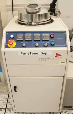
The Specialty Coating Systems PDS 2010 parylene deposition system provides users with reliable and repeatable conformal parylene coatings ranging from 75 micrometers down to a few nanometers thick. The system can accommodate substrates ranging from 200 mm diameter wafers down to small pieces.
Specifications/Capabilities
- Precursors supported:
- Parylene N.
- Parylene C.
- Thickness range: 75 µm to 10 nm.
Usage Information
Supported Sample Sizes
- Maximum wafer diameter: 200 mm (8 in).
- Small pieces supported: Yes.
- Maximum thickness: 1 mm.
Typical Applications
- Electronic and automotive applications.
- Biocompatible coatings for medical applications.
- Moisture and chemical barriers.
- Thin film dielectrics.
Created June 6, 2014, Updated March 4, 2025