
Official websites use .gov
A .gov website belongs to an official government organization in the United States.
Secure .gov websites use HTTPS
A lock (
) or https:// means you’ve safely connected to the .gov website. Share sensitive information only on official, secure websites.
Problem
Conventional Electron Spin Resonance (ESR) technologies can only claim to have detected the existence of a single defect with little understanding of the defect's identity. Additionally, each of these technologies has its own specific limitations, and all currently lack the ability to acquire precise spectroscopic information.
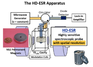
Invention
The new High Definition-E S R(HD-E S R ) spectrometer utilizes a superior detection scheme to perform electron spin resonance measurements. The major innovation centers on the use of a shorted coaxial “probe” (as small as a few nanometers) to excite the sample under test using near-field microwave radiation. This approach provides 10 orders of magnitude sensitivity improvement compared to conventional spectrometers. Another innovation is the use of a donut-shaped, small permanent magnet to create a highly uniform magnetic field for this very small probe. This greatly simplified technology can scan across a sample, producing spectroscopic and spatially determined atomic-scale defect information.
Potential Commercial Applications
The key breakthrough in HD-ESR is not the ability to measure single defects, but the ability to measure single defects with the comprehensive spectroscopic information necessary to understand their physical and chemical nature. It has a multitude of applications, e.g., anthropology, fuel science physiology, and meteorology.
Competitive Advantage
HD-ESR can laterally scan across the surface of any sample and characterize defects at or beneath the surface without making contact. For example, a fully active transistor can be probed with all the electrical connections in place. Transistor instabilities and/or performance degradation can be accurately linked to the presence and specific location of atomic-scale defects located within the active area of a highly scaled device. Detrimental fabrication processes can be easily modified to mitigate unwanted defect profiles and boost performance.