
Official websites use .gov
A .gov website belongs to an official government organization in the United States.
Secure .gov websites use HTTPS
A lock (
) or https:// means you’ve safely connected to the .gov website. Share sensitive information only on official, secure websites.
NanoFab Tool: Filmetrics F50 UV Mapping Reflectometer
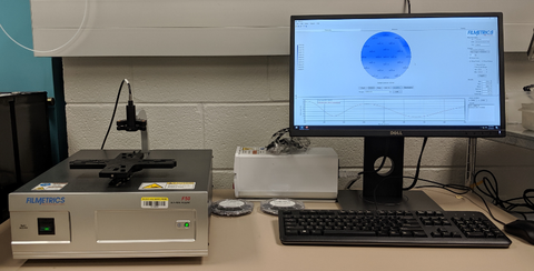
The Filmetrics F50 is an automated thin-film thickness mapping system equipped with a motorized r-theta stage that moves automatically to selected measurement points and provides thickness measurements as fast as two points per second. The system is capable of mapping wafers using predefined polar, rectangular or linear map patterns with center or edge exclusion.
Specifications/Capabilities
- Film thicknesses mapping of 100 mm (4 in), 150 mm (6 in), and 200 mm (8 in) diameter semi spec wafers.
- Automatic pattern generation of polar, rectangular or linear maps.
- User defined maps.
- Center or edge exclusion.
- Standard films:
- Oxide on silicon.
- Nitride on silicon.
- Polysilicon on oxide on silicon.
- Photoresist on silicon.
- Index of refraction and absorption determination (n and k).
- Small pieces supported: Yes
Typical Applications
- Thickness mapping of chemical mechanical polished thin films.
- Optical constants determination of deposited films.