
Official websites use .gov
A .gov website belongs to an official government organization in the United States.
Secure .gov websites use HTTPS
A lock (
) or https:// means you’ve safely connected to the .gov website. Share sensitive information only on official, secure websites.
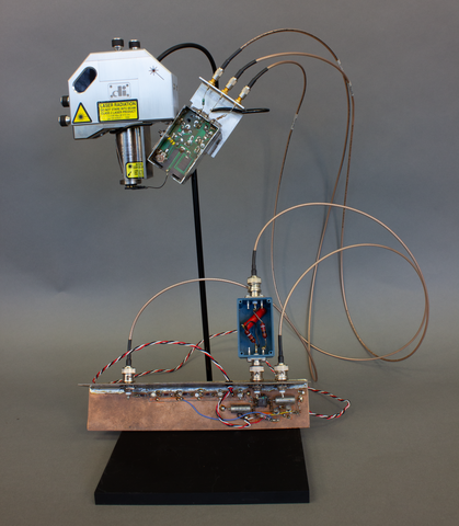
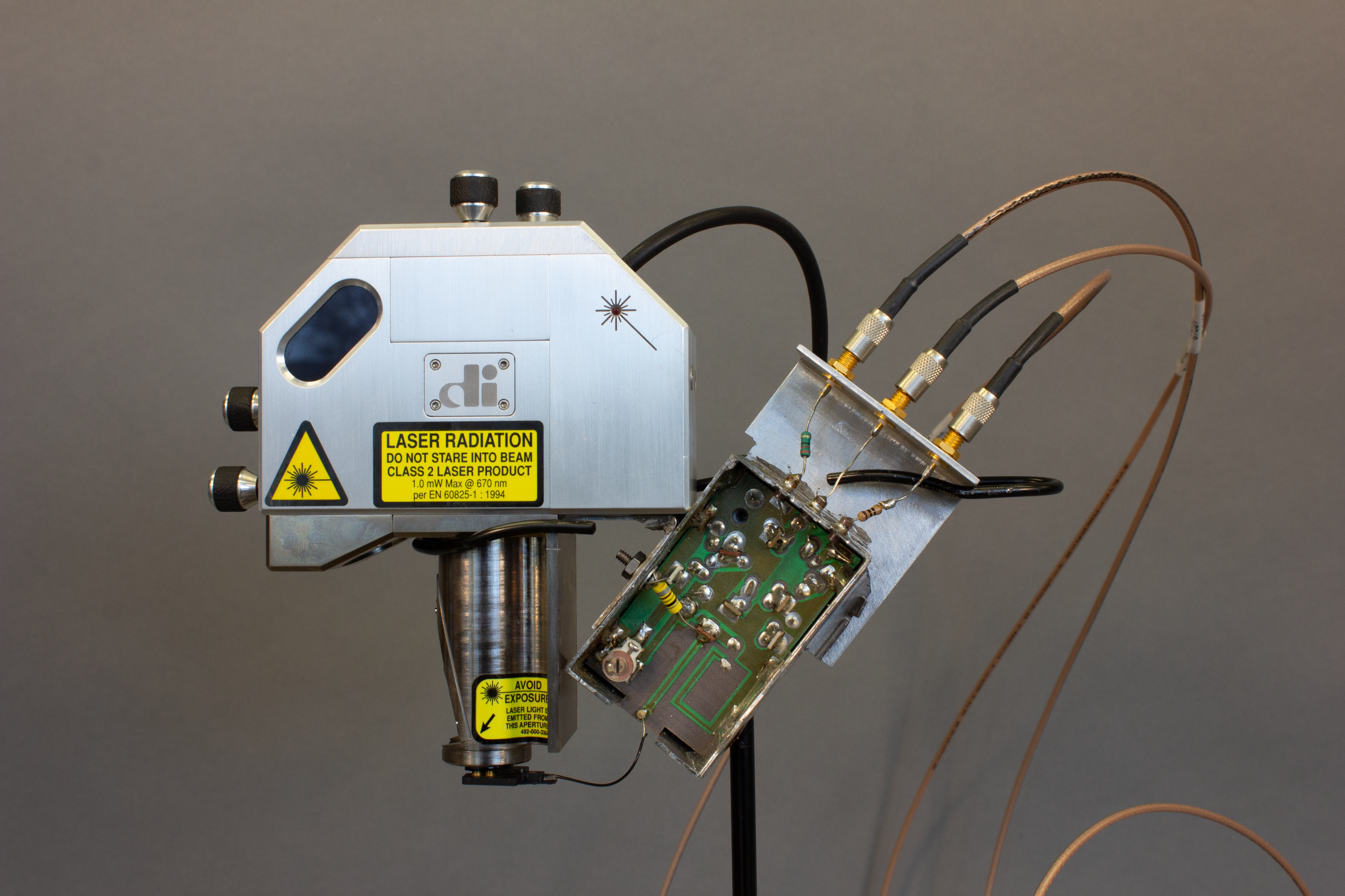
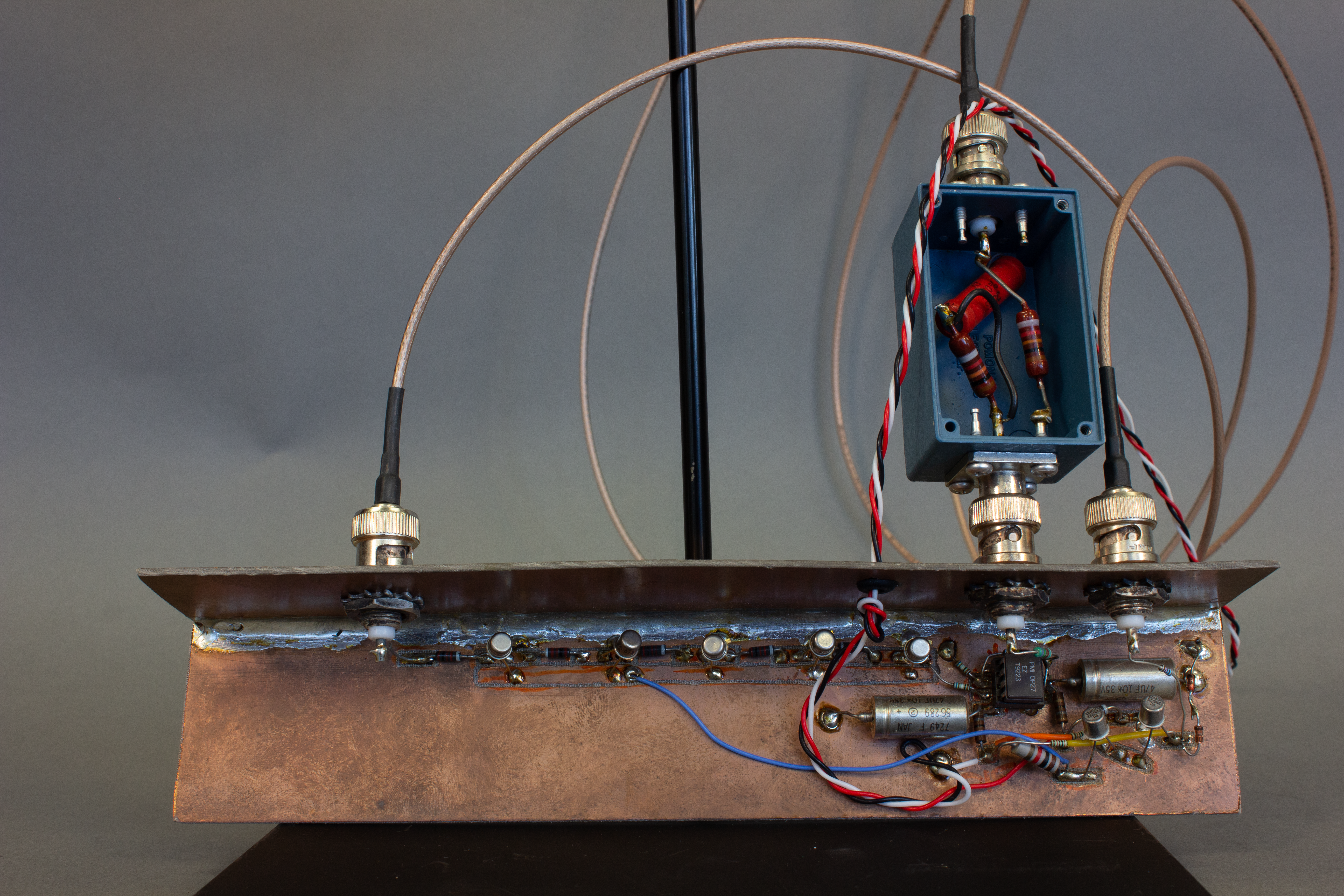
VideoDiscs and the Scanning Capacitance Microscope: A failed consumer product solves a semiconductor metrology challenge

In the early 1990s researchers in NIST’s Semiconductor Electronics Division repurposed the sensors from used Videodisc players, an unpopular home video system from the 1980s, to build an advanced measurement tool for the semiconductor industry.
A Commercial Failure
Videodiscs (or video discs) were a commercially unsuccessfully home video system produced by RCA from 1981-1986. The system used a stylus to read stored video capacitively (as differences in electrical charge) on a grooved disc that resembled a phonograph record. Overtaken in the consumer market by laserdiscs (which stored data optically) and VHS tapes (magnetic storage), videodiscs lost millions of dollars over its brief production run.
Repurposed for Success
Although videodisc technology failed in the consumer market, the capacitance sensors developed for these systems were highly sensitive instruments, capable of resolving capacitance differences of attofarads. In the 1980s researchers at RCA, and later at IBM, would repurpose this technology to create a Scanning Capacitance Microscope (SCM). When paired with existing Atomic Force Microscopes (AFM), highly sensitive capacitance measurements were possible in two-dimensions; down to 10 nanometers.
The SCM found an application as a solution to the two-dimensional dopant profiling problem in the semiconductor manufacturing industry. The properties and operation of semiconductors depend on the distribution (or profile) of the dopant atoms (intentionally added chemical impurities) in the device. Knowing this distribution is essential for process control and device modeling. Semiconductor manufacturers used secondary ion mass spectroscopy and spreading resistance to measure the dopant distribution in one-dimension (depth). By the late-1980s, semiconductors had become so small that 1D measurements were no longer sufficient and the industry needed two-dimensional methods (depth and lateral spread) to adequately characterize the dopant distribution to build the next-generation of advanced semiconductors.
NIST’s Role
Joseph Kopanski, Jay Marchiando and David Berning of the NIST Semiconductor Electronics Division used the capacitance sensors from old videodisc players to custom- build a series of SCMs beginning in the early 1990s. Their goal was to understand and explain the physics of this new instrument, determine how the measured capacitance between the AFM tip and a cross-sectioned semiconductor chip was related to the dopant distribution, and to provide industry with viable models and software to extract accurate two-dimensional dopant distribution from capacitance measurements.
Growth of an Industry
NIST’s validation of the SCM instrument concept and distribution of viable data acquisition and interpretation techniques enabled the commercial production of scanning capacitance microscopes and the development of more advanced semiconductors. The SCM and NIST’s techniques found wide application in integrated circuit process control and failure analysis laboratories. They were used to verify that semiconductor junctions were of the expected type, dimensions, and magnitude. Dopant distributions measured with the SCM were used in TCAD models of device performance. The SCM is now part of a semiconductor microscopy market that generates more than $100 million annually.
While semiconductors today are now three-dimensional and require 3D metrology, the SCM remains an important analysis tool for the integrated circuit industry and an active topic of instrument development.
References:
“Scanning capacitance microscopy.” J. R. Matey and J. Blanc. Journal of Applied Physics, Vol. 57, No.5, 1437 (March 1, 1985). p. 1437-1444. DOI: 10.1063/1.334506
“Scanning capacitance microscopy on a 25 nm scale.” C. C. Williams, W. P. Hough, and S. A. Rishton. Applied Physics Letters, Vol. 55, No. 2, (July 10, 1989.) p. 203-205. DOI: 10.1063/1.102096.
“Scanning capacitance microscopy measurements and modeling: Progress towards dopant profiling of silicon.” J. J. Kopanski, J. F. Marchiando and J. R. Lowney. Journal of Vacuum Science & Technology B: Microelectronics and Nanometer Structures Processing, Measurement, and Phenomena, Vol. 14, No. 1 242 (Jan-Feb 1996). p. 242-247. DOI: 10.1116/1.588455
“Scanning capacitance microscopy measurement of two-dimensional dopant profiles across junctions.” J. J. Kopanski, J. F. Marchiando, D. W. Berning, R. Alvis, and H.E. Smith, Journal of Vacuum Science & Technology B: Microelectronics and Nanometer Structures Processing, Measurement, and Phenomena, Vol. 16, No. 1, p. 339-343. (Jan-Feb. 1998); DOI: 10.1116/1.589807
Example of how to reference this exhibit:
NIST Museum. 2023. Videodiscs and the Scanning Capacitance Microscope. Gaithersburg, MD: National Institute of Standards and Technology. Online. https://www.nist.gov/nist-museum/videodiscs-and-scanning-capacitance-microscope-failed-consumer-product-solves
Author. Year. Exhibit Name. Place published: Publisher. Online. URL.