
Official websites use .gov
A .gov website belongs to an official government organization in the United States.
Secure .gov websites use HTTPS
A lock (
) or https:// means you’ve safely connected to the .gov website. Share sensitive information only on official, secure websites.
How Low Can You Go? Lower Than Ever Before
NIST scientists make most sensitive measurements to date of silicon’s conductivity for future solar cell, semiconductor applications.

Silicon, the best-known semiconductor, is ubiquitous in electronic devices including cellphones, laptops and the electronics in cars. Now, researchers at the National Institute of Standards and Technology (NIST) have made the most sensitive measurements to date of how quickly electric charge moves in silicon, a gauge of its performance as a semiconductor. Using a novel method, they have discovered how silicon performs under circumstances beyond anything scientists could test before — specifically, at ultralow levels of electric charge. The new results may suggest ways to further improve semiconductor materials and their applications, including solar cells and next-generation high-speed cellular networks. The NIST scientists report their results today in Optics Express.
Unlike previous techniques, the new method does not require physical contact with the silicon sample and allows researchers to easily test relatively thick specimens, which enable the most accurate measurements of semiconductor properties.
The NIST researchers had previously done a proof-of-principle test of this method using other semiconductors. But this latest study is the first time researchers have pitted the new light-based technique against the conventional contact-based method for silicon.
It’s too soon to say exactly how this work might be used someday by industry. But the new findings could be a foundation for future work focused on making better semiconducting materials for a variety of applications, including potentially improving efficiency in solar cells, single-photon light detectors, LEDs and more. For example, the NIST team’s ultrafast measurements are well-suited to tests of high-speed nanoscale electronics such as those used in fifth-generation (5G) wireless technology, the newest digital cellular networks. In addition, the low-intensity pulsed light used in this study simulates the kind of low-intensity light a solar cell would receive from the Sun.
“The light we use in this experiment is similar to the intensity of light that a solar cell might absorb on a sunny spring day,” said NIST’s Tim Magnanelli. “So the work could potentially find applications someday in improving solar-cell efficiency.”
The new technique is also arguably the best way to get a fundamental understanding of how the movement of charge in silicon is affected by doping, a process common in light sensor cells that involves adulterating the material with another substance (called a “dopant”) that increases conductivity.
Digging Deep
When researchers want to determine how well a material will perform as a semiconductor, they assess its conductivity. One way to gauge conductivity is by measuring its “charge carrier mobility,” the term for how quickly electric charges move around within a material. Negative charge carriers are electrons; positive carriers are referred to as “holes” and are places where an electron is missing.
The conventional technique for testing charge carrier mobility is called the Hall method. This involves soldering contacts onto the sample and passing electricity through those contacts in a magnetic field. But this contact-based method has drawbacks: The results can be skewed by surface impurities or defects, or even problems with the contacts themselves.
To get around these challenges, NIST researchers have been experimenting with a method that uses terahertz (THz) radiation.
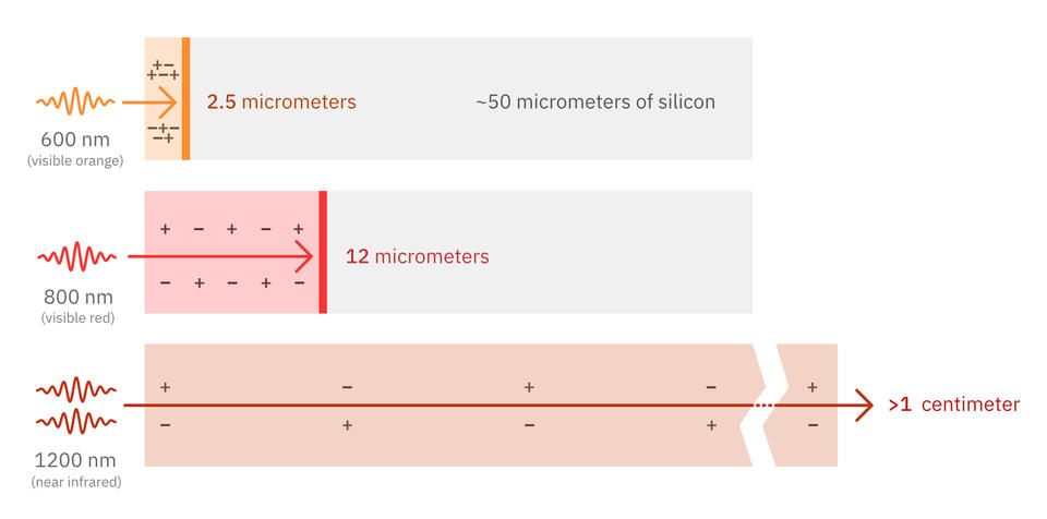
NIST’s THz measurement method is a rapid, noncontact way to measure conductivity that relies on two kinds of light. First, ultrashort pulses of visible light create freely moving electrons and holes within a sample — a process called “photodoping” the silicon. Then, THz pulses, with wavelengths much longer than the human eye can see, in the far infrared to microwave range, shine on the sample.
Unlike visible light, THz light can penetrate even opaque materials such as silicon semiconductor samples. How much of that light penetrates or is absorbed by the sample depends on how many charge carriers are freely moving. The more freely moving charge carriers, the higher the material’s conductivity.
“No contacts are needed for this measurement,” said NIST chemist Ted Heilweil. “Everything we do is just with light.”
Finding the Sweet Spot
In the past, researchers performed the photodoping process using single photons of visible or ultraviolet light.
The problem with using only one photon for doping, though, is that it typically penetrates only a small way through the sample. And since the THz light completely penetrates the sample, researchers can effectively use this method to study only very skinny silicon samples — on the order of 10 to 100 billionths of a meter thick (10 to 100 nanometers), about 10,000 times thinner than a human hair.
However, if the sample is that thin, researchers are stuck with some of the same issues as with the conventional Hall technique — namely, surface defects can skew the results. The thinner the sample, the bigger the impact of surface defects.
The researchers were torn between two objectives: Increase the thickness of the silicon samples, or increase the sensitivity they get from using single photons of light.
The solution? Illuminate the sample with two photons at once instead of one at a time.
By shining two near-infrared photons on the silicon, scientists are still only using a small amount of light. But it’s enough to get through much thicker samples while still creating the fewest possible electrons and holes per cubic centimeter.
“With two photons being absorbed at once, we can get deeper into the material and we can see a lot fewer electrons and holes generated,” Magnanelli said.
Using a two-photon measurement means the researchers can keep the power levels as low as possible, but still fully penetrate the sample. A conventional measurement can resolve no fewer than one hundred trillion carriers per cubic centimeter. Using its new method, the NIST team resolved a mere 10 trillion, at least 10 times more sensitivity — a lower threshold for measurement.
The samples studied so far are thicker than some other samples — about half a millimeter thick. That’s thick enough to avoid surface defect issues.
And in lowering the threshold for measuring free holes and electrons, the NIST researchers found a couple of surprising results:
Other methods had shown that as researchers create fewer and fewer electrons and holes, their instruments measure higher and higher carrier mobility in the sample — but only up to a point, after which the carrier density gets so low that the mobility plateaus. By using their noncontact method, NIST researchers found that the plateau occurs at a lower carrier density than previously thought, and that the mobilities are 50% higher than measured before.
“An unexpected result like this shows us things we didn’t know about silicon before,” Heilweil said. “And though this is fundamental science, learning more about how silicon works could help device makers use it more effectively. For example, some semiconductors may work better at lower doping levels than currently used.”
The researchers also used this technique on gallium arsenide (GaAs), another popular light-sensitive semiconductor, to demonstrate that their results are not unique to silicon. In GaAs, they found that the carrier mobility continues to increase with lower charge carrier density, about 100 times lower than the conventionally accepted limit.
Future NIST work might focus on applying different photodoping techniques to samples, as well as varying the samples’ temperature. Experimenting with thicker samples may provide even more surprising results in semiconductors. “When we use the two-photon method on thicker samples we may produce even lower carrier densities that we can then probe with the THz pulses,” Heilweil said.
-- Reported and written by Jennifer Lauren Lee
Paper: T. Magnanelli and E. Heilweil. Carrier Mobility of Silicon by Sub-Bandgap Time-Resolved Terahertz Spectroscopy. Optics Express. Published February 26, 2020. DOI: https://doi.org/10.1364/OE.382840