U.S. flag

An official website of the United States government

Official websites use .gov
A .gov website belongs to an official government organization in the United States.

Secure .gov websites use HTTPS
A lock ( ) or https:// means you’ve safely connected to the .gov website. Share sensitive information only on official, secure websites.

Engineering predictable behavior into GaN devices: An approach to accelerating design and optimization

GaN transistor circuit model

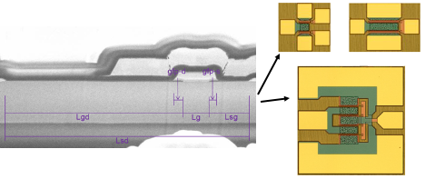
Thousands of transistors within unique devices having varied micrometer-scale physical dimensions were manufactured. The electron micrograph cross section (left) has many possible transistor designs (three examples at right) that were tested over many thermal and electrical loading conditions. See https://doi-org.wrs.idm.oclc.org/10.1016/j.jcrysgro.2019.04.008

Credit: Air Force Research Laboratory

Like the shift from propeller to jet power, gallium nitride (GaN) transistors promise more speed, power, and agility to everything emitting radio or microwave power: radar, electronic warfare, and communications systems. This comes with initial cost and reliability concerns, especially for the most risk-averse applications, because the new technology has different characteristics than the old.

The U.S. Department of Defense has developed a program in partnership with industry that endeavors to build a GaN transistor circuit model that covers a broad swath of process performance, design, and usage space to benefit the entire U.S. industrial base. In the spirit of the MGI, this program seeks to improve upon today's “point circuit models” that predict performance characteristics in a narrow electrical, thermal, and process range, and that rely on proprietary test datasets. Instead, this activity seeks to create a complete “computational toolset” that will include all relevant physical effects needed to fully model performance and reliability within the design phase and prior to expensive system integration.

This program has already successfully demonstrated the initial design toolset, capturing those effects for the first time for this industry, by implementing GaN physics of failure as part of the circuit design process to optimize a GaN device. Both circuit and system designs are included early in the design phase, with the primary objective of reducing the number of iterative design/build/test cycles, along with attendant reductions in development cost and time delays.

The integrated modeling tools that result from this program will enable the U.S. industrial base to more efficiently develop and deliver transformational capabilities to the U.S. Air Force.

Created September 2, 2021