
Official websites use .gov
A .gov website belongs to an official government organization in the United States.
Secure .gov websites use HTTPS
A lock (
) or https:// means you’ve safely connected to the .gov website. Share sensitive information only on official, secure websites.
NanoFab Tool: ADT 7132 Dicing Saw
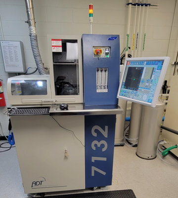
ADT 7132 Dicing Saw
The ADT 7132 dicing saw is used to cut multi-device substrates into individual chips. The system can accommodate substrates up to 1 mm thick and supports sizes ranging from small pieces to 300 mm diameter wafers.
Specifications/Capabilities
- Automatic mode for full wafer dicing.
- Measurement resolution: 0.1 µm.
- Positioning accuracy: 0.5 µm.
- Typical blade thickness (width of cut): 35 µm (45 µm) to 200 µm (240 µm)
Usage Information
Supported Sample Sizes
- Maximum wafer diameter: 300 mm (12 in).
- Small pieces supported: Yes.
- Maximum thickness: 1 mm.
Typical Applications
- Device separation after wafer processing.
- Dicing of silicon, glass, Pyrex, quartz, sapphire, lithium niobate and silicon carbide.
Created June 19, 2014, Updated August 25, 2025