
Official websites use .gov
A .gov website belongs to an official government organization in the United States.
Secure .gov websites use HTTPS
A lock (
) or https:// means you’ve safely connected to the .gov website. Share sensitive information only on official, secure websites.
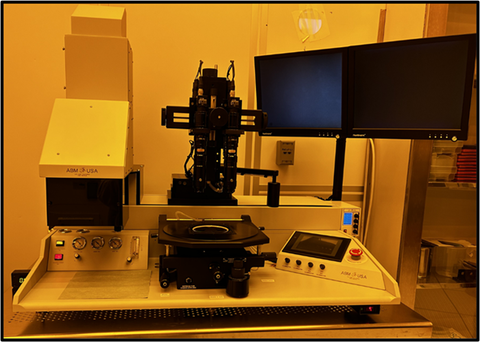
NanoFab Tool: ABM Mask Contact Aligner
Credit:
NIST
The ABM contact aligner allows users to align patterns on the front or back of a substrate and to print feature sizes down to 800 nm. The tool offers vacuum, soft, hard and flood exposure methods with frontside overlay accuracy better than 500 nm. It can accommodate substrates ranging from 150 mm diameter wafers down to small pieces.
Specifications/Capabilities
- Exposure methods: flood, soft, hard, and vacuum contact.
- Auto-Z Planarization, Wedge Compensation, and Leveling of Chuck
- Exposure wavelengths:
- 365 nm to 400 nm.
- 220 nm Wavelength Filter.
- 254 nm Wavelength Filter.
- Illumination area: 150 mm diameter.
- Resolution: 800 nm.
- Frontside and Backside Alignment.
- Frontside alignment accuracy: = 500 nm.
- Backside alignment accuracy: = 5 micrometer.
- Overlay accuracy: = 500 nm.
Usage Information
Supported Sample Sizes
- Maximum wafer diameter: 150 mm (6 in).
- Maximum substrate thickness: 6 mm.
- Small pieces supported: Yes.
- Mask sizes supported:
- 127 mm x 127 mm (5 inch).
- 178 mm x 178 mm (7 inch).
Typical Applications
- Medical devices.
- Biofluidic devices.
- Microelectromechanical systems.
- Thermal sensors.
- Printing micrometer size and larger features.
Created November 29, 2023, Updated March 3, 2025