Official websites use .gov
A .gov website belongs to an official government organization in the United States.
Secure .gov websites use HTTPS
A lock (
) or https:// means you’ve safely connected to the .gov website. Share sensitive information only on official, secure websites.
News and Updates
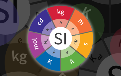
New Atom-Based Thermometer Measures Temperature More Accurately
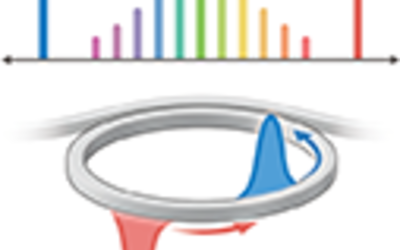
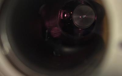
Researchers develop a new type of frequency comb that promises to further boost the accuracy of time keeping
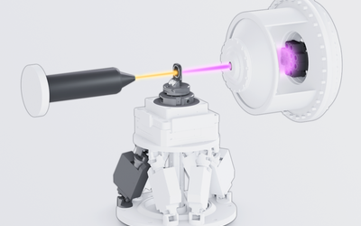
NIST Scientists Develop Novel CT Scan Device for Integrated Circuits
Blog Posts

Measurement in the Movies
Unidentified Museum Objects V