
Official websites use .gov
A .gov website belongs to an official government organization in the United States.
Secure .gov websites use HTTPS
A lock (
) or https:// means you’ve safely connected to the .gov website. Share sensitive information only on official, secure websites.
Amplifiers
Summary
To process information from quantum circuits and systems, it is important to have amplifiers with wide bandwidth, high dynamic range, and extremely low noise. Parametric amplifiers based on an inductance that varies with electrical current can satisfy these requirements.
Description
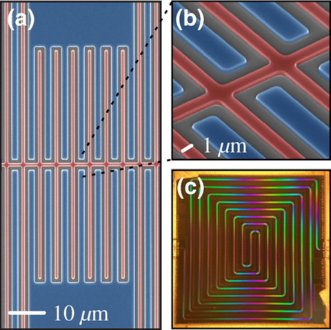
Micrographs of kinetic inductance-based parametric amplifier. (a) The transmission line of the amplifier (red) is periodically loaded with shorter fingers. (b) Line and fingers are 1 μm wide, and each cell is 5 μm long. (c) The overall KITWPA amplifier is laid out in a spiral configuration on a 2×2 cm chip that is clamped to a copper base.
We have developed parametric amplifiers based on two different technologies: Josephson Junctions and superconductors with high kinetic inductance, a representation of the kinetic energy of superconducting Cooper-pair charge carriers. Junction-based parametric amplifiers (JPAs) are well suited for measuring the smallest signals of interest such as signals from superconducting qubits. Kinetic inductance-based parametric amplifiers (KITWPAs) are well suited for higher power applications such as measuring the signals from arrays of cryogenic sensors. Both JPAs and KITWPAs can have noise levels near the quantum limit. We have also built frequency combs based on superconductors with high kinetic inductance.
Major Accomplishments
- Amplification and squeezing of quantum noise with a Josephson Parametric Amplifier
- Acceleration of axion searches using vacuum squeezing by Josephson Parametric Amplifiers
- Development of Kinetic Inductance Traveling-Wave Parametric Amplifiers with 50 Ohm intrinsic impedance
- Development of a three-wave mixing Kinetic Inductance Traveling-Wave Parametric Amplifier with near-quantum-limited noise performance
- Operation of a Kinetic Inductance Traveling-Wave Parametric Amplifier at 4 Kelvin
- Development of superconducting, broad-band microwave frequency combs