Taking Measure
Just a Standard Blog

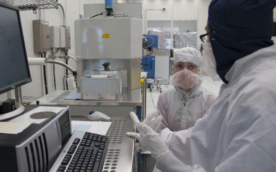
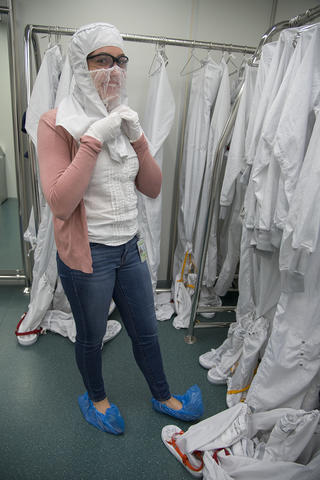
If I told you my job required a hair net, a “bunny suit,” and a million-dollar piece of equipment, would you have any idea what I do? Do I sound like a mad scientist or a crazy lunch lady? If you haven’t caught on yet, I’ll give you a hint: Don’t trust the mystery meat. Just kidding! I am actually an undergraduate student working in nanofabrication at NIST in the Summer Undergraduate Research Fellowship (SURF) program. I create and study devices on the nanoscale, which is 10^-9 meters, or for all you non-science types out there, we’re talking billionths of a meter.
Though I’m now studying in a very specialized field, when I started college, I wasn’t sure what path I would take. I had always been curious about how things worked and had a knack for science. With interests in anthropology and engineering, I signed up for classes in both but quickly realized I couldn’t pursue two majors. I settled on engineering and decided to take as many anthropology classes as I could fit in my schedule.
As I delved deeper into my engineering courses, I realized what I was looking for in anthropology could also be found in engineering. Engineering is about more than building bridges and cars; it’s about understanding how things work, how we’ve come this far in scientific understanding, and where we can go from here.

After deciding on engineering, I looked into ways to deepen my understanding of the field. My career options seemed as diverse as my course names (fluid mechanics, materials, aerodynamics, etc.), but I was an impatient, ambitious, and confused freshman, so I started going to professional events. At one, a professor talked about a new opportunity at my school—George Washington University—for a summer fellowship where I could research nanotechnology.
Before I could apply to the fellowship, I had to take a one credit class about nanotechnology. It was during this hour-long class that my interest was first spiked. In class, I learned about the ancient uses of nanotechnology, from stained glass to the way different sized nanoparticles of gold appear as different colors. I also learned about the future of nanotechnology applications like flexible electronics and invisibility cloaks.
In the lab, manipulating things on the atomic level gave me the ultimate level of understanding. Nanoscale science gave me an understanding of atomic-level behaviors and the ability to manipulate them. For this short class there were three professors who truly gave me my first taste of nanotechnology and engineering. Each one covered different aspects like the characterization and fabrication of devices, as well as the social and economic applications of nanotechnology to our everyday lives.
So, naturally, I applied to the nanotechnology fellowship and began my first experience conducting nanoscale research using electron beam lithography and a scanning electron microscope. I read research papers, participated in journal clubs, and fell under the spell of research.
I love doing research because it presents a riddle that you have to solve with your own knowledge and in collaboration with others. You could solve it in a day, a year, or longer. There is something addicting about generating ideas, testing them, failing—and then, ultimately, succeeding. Though I am new to research, I have learned to have patience—but I have a long way to go to truly get the hang of it!
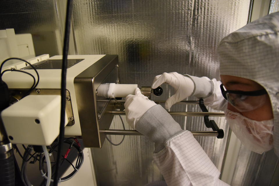
Once I found nanotechnology as the path to take with my engineering studies, I felt sure I could do this work for the rest of my life. In the spring of 2016, I applied to SURF and gladly accepted my position in April. Now, I’m spending every day in the beautiful Center for Nanoscale Science and Technology's NanoFab clean room at NIST fabricating new devices and gaining a greater understanding of what occurs on the nanoscale and the possibilities there. I feel honored to be able to work in a facility with state-of-the-art equipment and a great mentor to guide me along the way.

I am working this summer with Lei Chen on devising a new plasma etching process—a combination of atomic layer etching and another process called “Bosch” etching—to fabricate high-aspect ratio structures. High aspect ratio structures are characterized by a high ratio of the width to height—meaning they’re relatively tall, thin nanostructures. My job is to test different “recipes” for etching these structures.
The etching process starts with placing a patterned photoresist mask on top of a silicon wafer. You can think of the photoresist mask like a stencil. Then, we blast plasma onto the sample. The plasma reacts with the silicon, and the pattern from the mask is transferred to the wafer.
What we’re aiming for is high selectivity and a clean, straight etch. Selectivity is the ratio of how deep the silicon is etched with the pattern we want to how deep the mask is etched into. Higher selectivity is better because you can etch the silicon deeper before the plasma starts to destroy the photoresist mask. And a clean, straight etch is one that doesn’t have curves or jagged edges that would deform our structure.
So far, we’ve had some promising tests, and I’m excited to see where this project goes for the rest of the summer. Stay tuned to the blog for updates from me on my work this summer!


