
Official websites use .gov
A .gov website belongs to an official government organization in the United States.
Secure .gov websites use HTTPS
A lock (
) or https:// means you’ve safely connected to the .gov website. Share sensitive information only on official, secure websites.
Summary
Local material-property information is essential to evaluate emerging micro- and nanoscale materials, which many manufacturers would like to leverage for their unique properties and processing. Existing methods, however, lack spatial resolution and do not visualize the distribution in properties. Our goal is to develop and apply new scanning probe microscope (SPM) tools to rapidly map properties of materials with extremely high spatial resolution. Measuring localized variations in properties reveals material homogeneity and manufacturability challenges, and provides size-appropriate data critical for predictive modeling of device reliability and performance. Our research continually fluctuates between new measurement paradigms and cutting edge applications. This integration is facilitated by key expertise in SPM instrumentation, dynamics and electronics, coupled with application expertise ranging from advanced polymers to ferroelectrics.
Description
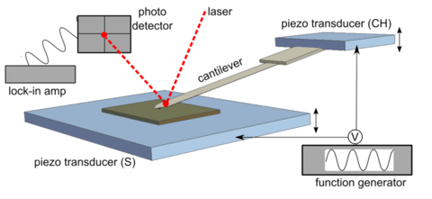
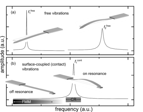
With a nanometer-sharp probe capable of delicate interaction with a limitless array of materials, SPM methods such as Atomic Force Microscopy (AFM) can aid in characterizing a wide range of materials in diverse environments from vacuum to biological serums. The atomic force microscope is operated in a number of modalities that seek to enhance sensitivity and aid in property quantification. Briefly, operating modes can be summarized as on- or off-resonance and either continuous-contact or intermittent-contact. Typical measurands include cantilever displacement, phase lag, resonance frequency and resonance quality factor. Such measurands are obtained under varying operating conditions such as applied electrical bias, then fed into a model of the cantilever mechanics or dynamics such that meaningful material properties may be obtained.
One of the first material properties pursued in the AFM was Young's modulus, which relates elastic stress and strain of the indenting AFM tip. Such mechanical measurements have been refined over the decade's since their initial invention, improving accuracy via improved hardware and data analysis. Mechanical properties have been further expanded by considering viscoelastic material characterization wherein he material dissipates energy during deformation, and typically exhibits a frequency dependent mechanical response. In addition to mechanical property information, the AFM can also measure electromechanical strain, adhesion, chemical structure, electrical conductivity, surface charge and more.
Our core expertise is the measurement and interpretation of resonant characteristics of the cantilever when in continuous contact (i.e. contact resonance force microscopy (CRFM)) with materials of interest. Here, the resonance serves as an amplifier to enhance sensitivity to spatial and temporal variations in material properties. We develop new operating modes to enhance the accuracy, sensitivity, speed, environment and delicacy of CRFM measurements. Many of our methods were initially developed for mapping viscoelastic heterogeneity of materials, but we have recently expanded our interests to temporal changes in material property arising from chemical reaction, and to the specific case of electromechanical strain mapping and quantification.
Major Accomplishments
Application: Photopolymer Additive Manufacturing
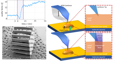
In photopolymer additive manufacturing (PAM), a liquid resin is selectively cured by a focused pattern of light, resulting in layer-by-layer formation of a solid 3D part. The method is attractive for commercial manufacturing because it affords a high degree of scalability towards higher-throughput and higher-spatial resolution; essential characteristics for critical applications such as biomaterials and metamaterials. During the voxel-scale liquid to solid reaction, the naive assumption is that only the area exposed to light experiences cure. In reality, a number of reactive and diffusive steps are competing at the length scale of the individual voxel, resulting in inaccurate representation of the input digital 3D model, and often widely varying mechanical properties that undermine reliability. By using the AFM probe as an in-situ photorheological sensor, we can map out the spatial variations in cure with time resolution much faster than the cure step, and spatial resolution much finer than the voxel itself. Rheological properties are recorded by monitoring the resonance frequency and quality factor of the cantilever during cure reaction, for different locations relative to the light source.
Callie I Fiedler‐Higgins et al Monitoring Fast, Voxel‐Scale Cure Kinetics via Sample‐Coupled‐Resonance Photorheology 2019 Small Methods 3 1800275
Application: Bias Induced Strain (Piezoresponse and related phenomena)
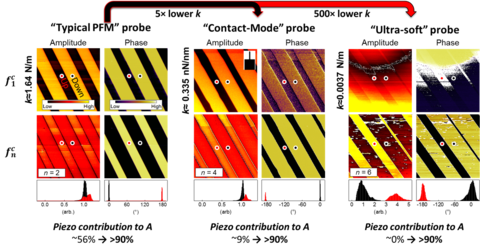
For a number of technologically important materials such as antennae, actuators, energy harversters, molecular machines and batteries, performance can be directly or indirectly tied to the relationship between applied bias voltage and material strain. With the AFM serving as an electrode to apply the bias, this strain can be measured directly from the deflection of the AFM cantilever, with nanometer spatial resolution. CRFM can be used to amplify the surface motion by a factor roughly equal to the quality factor. Typically, the use of CRFM in bias induced strain measurements has been met with many tradeoffs in inability to quantify and susceptibility to cross-talk and artifacts. We have been using our experience in CRFM viscoelastic measurements to systematically improve these short comings of CRFM bias induced strain measurements. In particular, we have worked on application of higher cantilever eigenmodes to enhance sensitivity and suppress ubiquitous electrostatic artifacts, application of cantilever vibrational shape characterization to quantify the true surface displacements, and application of a new method called isomorphic-CRFM that seeks to eliminate many forms of cross-talk.
Associated Product(s)
Project Summary (PDF)