
Official websites use .gov
A .gov website belongs to an official government organization in the United States.
Secure .gov websites use HTTPS
A lock (
) or https:// means you’ve safely connected to the .gov website. Share sensitive information only on official, secure websites.
Platforms for measuring properties of electrically addressable semiconductor nanocrystals
Summary
In measuring performance of submicron optoelectronic devices, such as lasers or light-emitting diodes (LEDs), conventional methods are limited to extrapolations from measurements on ensemble of nanocrystals or measurements based on a very limited number of nanocrystals. This limitation is independent of the spatial resolution of the used analytical instrument and is due to inability of the current methods to electrically access individual nanocrystals on a scalable style. In this project we are developing techniques to measure local properties of semiconductor nanocrystals in large size hierarchies. Our approach is based on “electrically addressable semiconductor nanocrystals” so they can be electro-optically probed. Such platforms are, especially, important in further development of emerging optoelectronic devices such as optical interconnects in nanoelectronics, visible light communication, and on-chip optical/chemical metrology and sensing.
Description
To determine electro-optical performance of nanocrystals with different surface registries in an ensemble, we have developed strategies to control two key parameters including spatial distribution and orientation of nanocrystals. This allows to electrically probe semiconductor nanocrystals from specific crystal facets. This ability was essential in revealing a previously unseen property in wide band gap (WBG) materials that can eliminate the decline in efficiency of LEDs (see section 1, below). Below are some of our research directions:
Model systems with superior efficiency:
- Exploring droop-free light-emitting diodes (LEDs)
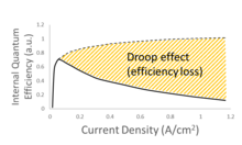
One of the significant challenges facing LED technology is the “efficiency droop”, which is the decline in internal quantum efficiency (IQE) with increasing current density. This phenomenon has limited the performance of all commercially available LEDs (Figure 1). The mechanisms causing efficiency droop have been among the most heavily investigated topics in the WBG materials and been linked to Auger recombination, phase space filling, stimulated emission, delocalization-activated nonradiative recombination, and incomplete carrier localization.
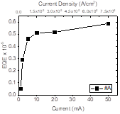
Using the developed “electrically addressable semiconductor nanocrystals” platform we have shown that droop-free is a shape dependent effect and fin shape semiconductors can eliminate this effect (figure 2).
 We have also shown that a fin shape semiconductor nanocrystal can substantially suppress the Auger recombination and the optical loss in a nanoscale LED. This property has resulted in driving LEDs to lasers at current densities more than 1000,000 mA/cm2 without any decline in efficiency.1 We have shown these light sources can generate microwatts of power (Figure 3), i.e., 100 to 1000 times more than any electrically driven submicron light source.
- UV-C LEDs for disinfection:
One of the important areas is increasing the brightness of UV-C LEDs beyond their current milliwatt power output with applications in multicolor fluorescence detection of pathogens as well as more effective UV-C light sources for disinfection of harmful pathogens.
- High-brightness sub-micron lasers (UV-near IR):
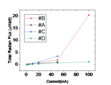
Figure 3. Examples of output power range of fin LEDs. The highest point in this graph corresponds to a fin laser.
Until now, the low efficiencies of LEDs have limited the output power of sub-micron LEDs and lasers to nanowatts, which is not adequate for practical applications including on-chip optical or chemical sensing. Fin LED/lasers offer new opportunities for developing a wide range of novel architectures for a broad range of applications. Our current focus is on developing methods that allow further reducing the footprint of such light sources, while developing mechanisms to control their basic properties such as brightness, stability, etc. These results will be key in developing models that can assist technology developers for developing advanced functionalities such as pulsed lasing, radiation hard devices and high temperature LEDs and lasers.
- Affordable nanomanufacturing:
Another roadblock in development of sub-micron light sources is that current methods of nanofabrication for small research and development volumes and entry into industrial manufacturing, are often cost-prohibitive. This is due to the high cost of controlling growth at the nanoscale. One of the advantages of our measurement platform is that it allows wafer scale fabrication of electrically addressable nanocrystal devices. This is because we use a low cost 2 mm-resolution optical lithography to create and control the growth of sub-micron nanocrystals.