Summary
This project aims to develop rigorous measurements and methodology needed for determining optical and electrical properties of advanced materials that might be employed for emerging advanced electronic and optoelectronic devices.
Description

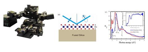
Spectroscopic ellipsometry measurement of a 2D monolayer and the optical property for such a thin layer.
Today's electronics have reached a point where sheer computation power has combined form and function as the key driver of large consumer markets. The demand for portable and pervasive electronics with greater functionality promises significant changes over the next decades in how society interacts with each other and its surroundings. Such rapid and significant change requires continued improvements in traditional high-performance low power electronics for informatics. These changes are also needed in entirely new device technologies based on emerging electronic materials as well as in novel integration methods to provide the specific functionality in the compliant form factor demanded. Examples of these new electronic materials and devices include 2-D heterostructure semiconductors, III-V, and metal oxide-based transistors, optoelectronics, and sensors. As new concepts are being developed and demonstrated, a close coupling of technology and metrology development is also needed to continue to solidify our understanding and ensure a smooth transition to commercialization.
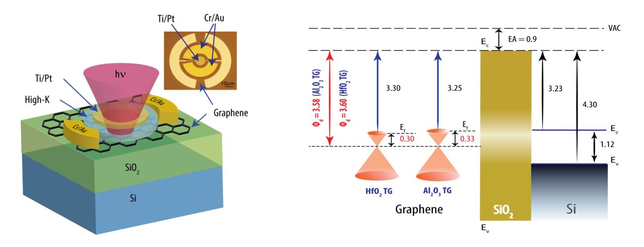
In this project, we advance measurement science that precisely determines band alignment/offset at buried heterojunction interfaces and governs device operation in advanced ultra-low power high performance transistors. We develop novel methods and test structures to characterize the electromagnetic response of emerging atomic layer 2-D electronic materials over a broad spectral range for the design of advanced electronic/optoelectronic devices and which are critical to the stringent demands of process control in eventual manufacturing environments. Our main metrology techniques employed in this project involve wide spectral range ellipsometry and a unique internal photoemission spectroscopy. Currently under construction is an effort to design and implement an automation of 2D exfoliation which involves machine learning and single and multiple small exfoliated 2D flakes that will facilitate and expedite the multi 2D layer heterostructure fabrication process that will certainly become a major part in the design of advanced electronic and optoelectronic devices.
Broad band spectroscopic ellipsometry measurements for optical properties and layer structure
A combination of spectroscopic ellipsometers (Fig. 1) with focusing capability and spectral range covering from 148 nm to 1.700 mm allows the determination of optical properties of single and multiple layer structures down to monolayer thickness. The information obtained on this stack of thin films includes film thickness, uniformity, composition, surface roughness, optical and electronic band transitions, and optical band gaps. The focusing and fast scanning capability also allow the determination of these parameters across a sample to a resolution of ≈150 mm. The fast scanning mode also facilitates the monitoring of the sample dynamics.
Internal Photoemission measurements for electronic band alignments
Internal photoemission (IPE) is used to determine the energy barrier height at the solid/solid interface. Early work has impacted the research efforts to integrate high-k dielectrics and metal gates where IPE contributed to the understanding of the barrier height related to leakage current in a corresponding transistor. Currently, the effort has been refined and tuned to more difficult material structures, such as 2D single layers where we have demonstrated IPE capabilities to handle the band offset measurements of various MX2 semiconductors (M = Mo, W; X = S, Se) which have brought new possibilities for future electronic and optoelectronic applications.


