
Official websites use .gov
A .gov website belongs to an official government organization in the United States.
Secure .gov websites use HTTPS
A lock (
) or https:// means you’ve safely connected to the .gov website. Share sensitive information only on official, secure websites.
Summary
Develop critical thermal and electrical transport measurement methods, instrumentation, and reference materials needed to support the development, performance, and reliability of bulk and thin film materials used in semiconductor microelectronics and energy conversion applications.
Description

The image above is an exploded cross section diagram representing the simplified structure layers in a MOSFET transistor. Thermoreflectance (TR) laser-based measurement techniques, a key focus of this project, can measure the thermal properties of substrates, thin films, multilayer structures, and their interfaces.
The properties of materials and interfaces that govern reliability, performance, and thermal transport in advanced microelectronic packages are not fully characterized or understood, especially at device length scales wherein properties may differ significantly from bulk or literature values. Thermal management is critical for microprocessors and for wide bandgap semiconductor devices used for energy conversion applications (inverters, AC/DC-DC converters, solid-state lighting, RF, and communication devices). The demand for increased performance in high power density and hierarchically complex semiconductor devices has outpaced the development of measurement techniques and reliable thermal property data needed to effectively design, model, and evaluate advanced microelectronics.
Thermal property measurements
This project will improve thermal property measurements for multilayer semiconductor materials and generate reliable data that feeds into thermal simulations of integrated chips and power electronics. Leveraging our existing expertise and collaborations with instrument vendors and the semiconductor industry, we will validate and improve emergent thermal property measurement instrumentation and methods, provide on-demand data, and develop thermal conductivity reference standards.
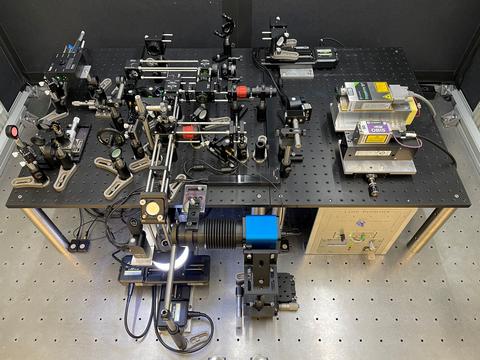
Our custom Frequency Domain Thermoreflectance (FDTR) instrument can provide rapid and reliable in situ thermal property data for materials that comprise fully packaged architectures, including: substrates, encapsulants, infills, thermal interface materials, bond layers, heat spreaders, as well as the traditional semiconductors, metals, and dielectrics. FDTR is a non-contact, modulated pump-probe technique that can measure thermal properties at length scales ranging between tens of nm to mm. A modulated laser periodically heats the surface and the multilayer stack, inducing a corresponding periodic change in surface reflectivity; the relative phase from a reflected probe beam is measured using a lock-in amplifier. Thermal conductivity, heat capacity, and thermal interface resistance of multilayered materials can be obtained through modeling a fit of the phase change of a reflected probe beam vs. the modulation frequency of a pump beam, where the probe and pump are coaxially focused on an Au reference layer/sample layer stack. The sample stage accommodates 76.2 mm DIA thin films, multilayer systems, or bulk samples; property maps can be obtained using the XY scanning platform. The entire measurement is automated using custom LabVIEW code, optical component flippers, and motorized stages.
Thermoelectric Measurements
Thermoelectric effects enable the inter-conversion of thermal and electrical energy, with applications that include solid-state waste heat recovery in engines for automotive and industrial manufacturing; power generation for aerospace, non-terrestrial exploration, and remote sensing; and refrigeration for consumer products, optical components, and microelectronics. This project provides the underpinning measurement science needed to support the development, production and reliability of materials and devices related to advanced energy sources, energy storage and energy-harvesting. We develop Standard Reference Materials (SRMs), measurement methodologies, comprehensive data sets, and phase equilibrium data for bulk and thin film thermoelectric materials that enable the reliable inter-laboratory comparison of data and the confirmation of reported high efficiency thermoelectric materials.
Associated Product(s)
SRM® 3451, “Low-Temperature Seebeck Coefficient Standard (10 K to 390 K)"
SRM® 3452, “High-Temperature Seebeck Coefficient Standard (295 K to 900 K)"