
Official websites use .gov
A .gov website belongs to an official government organization in the United States.
Secure .gov websites use HTTPS
A lock (
) or https:// means you’ve safely connected to the .gov website. Share sensitive information only on official, secure websites.
Problem
Patent Description
Detection of chemical species in air, such as industrial pollutants, poisonous gases, chemical fumes, and volatile organic compounds (VOCs), is vital for the health and safety of communities around the world. The development of reliable, portable gas sensors that can detect harmful gases in real-time with high sensitivity and selectivity is therefore extremely important.
Due to their small size, ease of deployment, and low-power operation, solid-state thin film sensors are favored over analytical techniques such as optical and mass spectroscopy, and gas chromatography for real-time environmental monitoring. Selectivity, which is a sensor's ability to discriminate between the components of a gas mixture and provide detection signal for the component of interest, is an important consideration for the sensor's real-life applicability. Conventional metal-oxide based thin film sensors, despite decades of research and development still lack selectivity for different species and typically require high working temperatures. As such, the usability of such conventional sensors is severely limited and poses long-term reliability problems.
For a chemical sensor, the active surface area is an important factor for determining its detection limits or sensitivity. It is known that the electrical properties of nanowires (NWs) change significantly in response to their environments due to their high surface to volume ratio. NWs are therefore well suited for direct measurement of changes in their electrical properties (e.g. conductance/resistance, impedance) when exposed to various analytes. Substantial research has demonstrated the enhanced sensitivity, reactivity, and catalytic efficiency of the nanoscale structures.
There have been attempts to demonstrate sensors based on nanotube/nanowire decorated with nanoparticles of metal and metal-oxides. Although such results demonstrate the potentials of the nanowire-nanocluster based hybrid sensors, fundamental challenges and deficiencies in such prior attempts remain. Most of the results provide for mats of nanowires. Although such mats may increase sensitivity, the complex nature of inter-wire conduction makes interpreting the results difficult. Also, room-temperature operation of such previous sensors has not been demonstrated, and the selectivity is shown for only a very limited number of chemicals. Conventional sensor devices require high operating temperatures (250°C.) and large response times (more than 5 minutes). Indeed, such temperature-assisted sensors typically provide for an integrated heater for the device. Further, the reported sensitivities of such conventional devices were quite low even with long response times. Further, such conventional devices typically do not provide for air as the carrier gas. However, the ability of a sensor to detect chemicals in air is what ultimately determines its usability in real-life.
Past demonstrations have resulted in poor selectivity of known chemical sensors, and therefore have not resulted in commercially viable gas sensors. For real-world applications, selectivity between different classes of compounds (such as between aromatic compounds and alcohols) is highly desirable. For example, the threat of terrorism and the need for homeland security call for advanced technologies to detect concealed explosives safely and efficiently. Detecting traces of explosives is challenging, however, because of the low vapor pressures of most explosives. Moreover, the difficulty of explosive detection is aggravated by the noisy environment which masks the signal from the explosive, the potential for high false alarms, and the need to determine a threat quickly. As such, trained canine teams remain the most reliable means of detecting explosive vapors to date; however, dogs are expensive to train and tire easily.
An ideal chemical sensor would be able to distinguish between the individual analytes belonging to a particular class of compounds, e.g. detection of the presence of benzene or toluene in the presence of other aromatic compounds, detection of a particular explosive compound, detection of a particular alcohol, etc. This is extremely challenging as most semiconductor-based sensors use metal-oxides (such as SnO2, In2O3, ZnO) as the active elements, which are limited due to the non-selective nature of the surface adsorption sites. The surface/adsorbate interactions of conventional sensor structures are limited and non-specific. Thus, conventional sensor devices lack the same selectivity as their bulk-counterpart devices.
Accordingly, there is a need for a nanostructure sensor device that solves one or more of the deficiencies of conventional devices. This invention does just that.
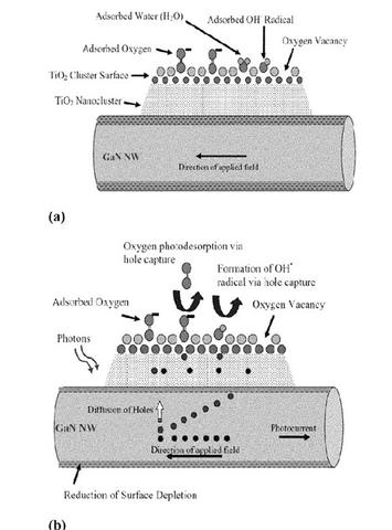
Description of the illustration below: Plates (a) and (b), are schematic representations of a GaN (Nanowire)-TiO2 (Nanocluster) hybrid sensor according to the present invention. FIG. 1, plate (a) shows the sensor in the dark showing surface depletion of the GaN nanowire, and FIG. 1, plate (b) shows the sensor under UV excitation with photodesorption of O2 due to hole capture.
Invention
A nanostructure sensing device comprises a semiconductor nanostructure having an outer surface, and at least one of metal or metal-oxide nanoparticle clusters functionalizing the outer surface of the nanostructure and forming a photoconductive nanostructure/nanocluster hybrid sensor enabling light-assisted sensing of a target analyte.
Features
The present invention is directed to highly selective and sensitive sensor devices including semiconductor nanostructures decorated with metal and/or metal-oxide nanoclusters or particles. The disclosed sensors provide numerous advantages over conventional sensors including: 1) light-induced room-temperature sensing as opposed to thermally induced sensing, providing for reliable operation at low-power, longer lifetime, and fast response/recovery time; 2) excellent selectivity of sensing of selected compounds (e.g., sensors able to distinguish toluene from other aromatic compounds); 3) wide sensing range (50 ppb-1%); 4) fast response and recovery; and 5) reliable and repeatable operation.