
Official websites use .gov
A .gov website belongs to an official government organization in the United States.
Secure .gov websites use HTTPS
A lock (
) or https:// means you’ve safely connected to the .gov website. Share sensitive information only on official, secure websites.
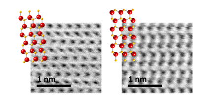
Scanning transmission electron microscopy annular dark field images images of a GaN film (left) and GaN nanowire (right) showing aligned columns of N atoms (yellow) and Ga atoms (red). The film is Ga-polar and the nanowire is N-polar. The slight lateral mis-registry between atom positions in the image and model for the left hand image is due to sample drift.
Many people who have heard of gallium nitride (GaN) know it as the semiconductor used in bright light-emitting diodes for flashlights and energy-efficient light bulbs. Those commercially important applications are based on thin (planar) films. But by the same growth method of slow deposition of gallium and nitrogen atoms to form successive layers, GaN can also be synthesized as three-dimensional (3D) nanostructures, which hold promise for many potential applications.
These 3D structures, often called GaN nanowires, are being developed by industry to improve LED efficiency for general lighting sources; and university and government laboratories are exploring their use in more advanced devices such as nanoscale light sources and single-photon sources for quantum information systems.
Until recently, however, there were no direct methods to determine a critical property of GaN – its "crystal polarity" – which has a profound impact on synthesis, materials characteristics, and device performance. Now NIST scientists have measured that property using a newly acquired instrument, and found that the nanowires grow with an inverted polarity relative to conventional planar material for LEDs.
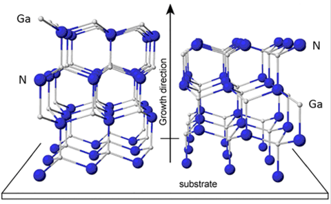
Unlike most semiconductors, the GaN crystal lacks symmetry along one of its axes. This asymmetry, called crystal polarity, is illustrated in the figure below left, which shows two different orientations, or polarities, of gallium atoms (white) and nitrogen atoms (blue). Control of this inherent asymmetry in planar layers and 3D nanostructures is critical to the manufacture of highly ordered nanowire arrays.
"Flipping the crystal vertically puts the other polar surface on top," said Kris Bertness of NIST's Physical Measurement Laboratory. "So one way to think of this property is that we need to know which end is up. But because most GaN is grown as a thin film on wafers of a different material, such as silicon, changing polarity is not a simple matter of flipping the crystal because only one of the faces is exposed."
To make direct measurements of the crystallographic polarity of GaN films and nanowires, the NIST researchers used a new scanning transmission electron microscope (STEM) to image the Ga and N atom locations with atomic precision. This measurement requires the high resolution only recently attainable with STEM when instruments with aberration-corrected probes became available in the last five years.
The instrument has a resolution of 82 picometers (pm, 10-12 m). For comparison, covalently bonded gallium and nitrogen atoms are about 120 pm and 70 pm wide respectively.
The instrument also has a specialized detector, called an annular bright field detector, which allows imaging of light elements such as nitrogen. These capabilities are critical for the polarity imaging and were not previously available at NIST.
Although common manufacturing methods for GaN generally produce layers that are mostly of one polarity, they frequently contain small regions of the opposite polarity, called "inversion domains."
These domains behave as defects, causing poor control of electrical conductivity and problems during device fabrication. Polarity inversion also has a dramatic effect on amount of magnesium (Mg) that can be incorporated in GaN. Mg doping is essential for producing electrically positive ("p-type") areas in the crystal.
Regions with Ga-polar orientation during growth can incorporate over 10 times as much Mg. Inversion domains of N polarity are much more resistive and cannot efficiently produce light. Thus the efficiency of an LED is reduced directly in proportion to the fraction of inverted material. But because GaN planar layers also suffer from high densities of structural defects, it is difficult to identify the cause of poor efficiency without a diagnostic that can see both polarity and crystal defects. NIST's new aberration-corrected TEM can do both.
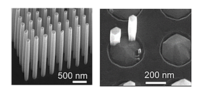
One method for eliminating crystal defects is to grow arrays of very small crystals, or nanowires, instead of a thin film. Perfect crystals are the most stable arrangement of atoms, and thus small crystals grown slowly will usually achieve perfection. Researchers have known for several years that two types of GaN nanowires form with different shapes and growth rates, and these were presumed to correspond to the two possible crystal polarities. But until direct TEM imaging of polarity was applied to this problem, no one could confirm this hypothesis or know which polarity corresponded to which type.
"In fact, the traditional method of determining GaN polarity by TEM, called convergent beam diffraction, has given misleading results when applied to nanowires," says Alexana Roshko, who performed the TEM direct imaging analysis. The ability to directly image sample polarity has accelerated the development of selective-area GaN nanowire arrays grown on polarity-controlled nucleation layers, resulting in engineering-level control over nanowire location and diameter.
"We now know that N-polar nanowires grow faster than Ga-polar nanowires," says Matt Brubaker, one of the researchers studying GaN nanowires in PML. Uniform polarity leads to homogeneous nanowire arrays with uniform length, which is critical for any device in which many nanowires will operate in parallel.
For example, when operating a large array of nanoLEDs as an LED chip, a uniform voltage will be applied across all the nanowires. If some of the nanowires are too short or too resistive, the electrical power will bypass them and only activate neighboring nanowires, and the overall device efficiency will suffer.
""Now that we have a reliable primary method of determining GaN polarity with high spatial resolution," Brubaker said, "we are also using this TEM method to develop faster, more convenient methods that use scanning probes and require less sample preparation."