
Official websites use .gov
A .gov website belongs to an official government organization in the United States.
Secure .gov websites use HTTPS
A lock (
) or https:// means you’ve safely connected to the .gov website. Share sensitive information only on official, secure websites.
Electrical Performance Measurements of Photovoltaics and Wide Band Gap Semiconductors for Power Electronics
Summary
A significant source of generated power for residential, commercial and small-system applications today are supplied by solar photovoltaic (PV) systems. PV offers a great choice for powering needs of small or large systems due to ease of integration, reliability, long safety track record and significantly reduced costs in recent years. Growth of PV, especially for space and internet-of-things (IoT) power applications requires new measurement scales and characterization methods. Furthermore, semiconductors for power applications, such as rectifiers, inverters, and voltage converters require more testing and characterization to assess their reliability in critical applications such as microinverters, traction motors [1] and artificial intelligence (AI) servers. Recently, we created a PV calibration service to help aid industry in performing SI-traceable low-uncertainty electrical performance measurements of photovoltaic cells and modules. Relying on lessons learned from this measurement service, we will pursue developing other measurement services and will participate on standard committees to help craft new standards on PV characterization, particularly under non-standard reporting conditions. In addition to maintaining and providing this measurement service, research work will focus on defect-related characterization of both PV and semiconductor materials for power electronics applications. A variety of novel characterization methods, including luminescence imaging techniques on materials such as perovskites, silicon carbide (SiC), and gallium nitride (GaN) will be deployed for this purpose. What will be learned from these measurements can be applied to defect metrology for all sorts of semiconductors of the future and will be important for understanding reliability issues in these materials.
Description
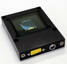
A NIST-fabricated/calibrated reference photovoltaic device (SRI 6014)
Objective
To develop or improve the electrical and optical measurement science of photovoltaic and power semiconductor materials and devices by: (1) providing a calibration service to allow industry and academia to accurately assess device performance under a range of operating conditions, (2) exploring the impact of defects in semiconductors using the novel techniques of electroluminescence and photoluminescence with two world-class NIST hyperspectral imagers, and (3) investigating performance and reliability of power electronics systems based on new wide bandgap semiconductors.
Technical Idea
To improve and implement state-of-the-art methods for characterizing power electronics components and PV cells and modules. The focus is to understand the role of defects on overall device performance, understand device reliability, and develop standard reference instruments, measurement services and new standards for the latest challenges in this field. NIST has been successful in developing a variety of advanced opto-electronic characterization techniques that have led to offering the PV SRI 6014 (see NIST SRI 6014.) and related measurement services. More recent technical work is related to advanced electrical characterization, and novel hyperspectral imaging techniques such as electroluminescence and photoluminescence. These techniques allow for visualization of the location and extent of electronic-grade defects within the semiconductor active layer in semiconductor devices and determine the nature and impact of their presence. Therefore, this project offers both measurement services to NIST customers and high-quality, high-impact journal articles and other publications to advance the current knowledge in these areas.
Research Plan
The PV SRI and calibration service continues to grow and generate interest in the community, particularly in the new areas of indoor photovoltaics and space PV. We offer this calibration service by maintaining the measurement systems, performing regular calibrations of equipment, and publicizing the NIST PV reference cells to a greater degree, highlighting the great selection of reference PV materials that are now available for customers. For indoor PV, further work can be done in standards and codes, particularly in tandem with external collaborators. A recently approved IEC standard has been shown to be inadequate and deficient in many ways [2], and we would like to continue working with several collaborators in authoring papers and reports that outline these deficiencies and propose improved solutions. We have had recent dialogues with other national metrology institutes, discussing ways we can work together to improve measurement protocols or standards, and we will pursue some of these topics in FY26. Also, at least one interlab-comparison will be organized and conducted with an international partner.
In FY 20, our new hyperspectral imaging system was used extensively for the first time to measure PV luminescence data on (mostly) multijunction solar cells in electroluminescence mode. The results of these early measurements were encouraging, and we performed baseline calibration measurements to obtain absolute electroluminescence data. In FYs 21 through 24, we focused on performing extensive electroluminescence and photoluminescence measurements using the hyperspectral imager on a variety of PV materials including GaAs and CdTe PV films or devices. With the delivery of a new optical cryostat in FY 21, we have been able to carry out these measurements as a function of temperature down to 77 K using liquid nitrogen. Measurements at such low temperatures have revealed novel, previously unexplored phenomena in some devices that could be important for understanding reliability issues for these materials in cold conditions such as deployment in space satellites. We intend to continue these temperature-dependent measurements into FY26 with new perovskite solar cells provided to us by two important collaborators, the University of Toledo and the Korea Research Institute of Chemical Technology. These new measurements will increase our scientific understanding of defects and shunts in these materials and will shed light on charge carrier transport phenomena in these devices.
Another research topic where electroluminescence imaging is important for understanding of defects, local damage, and failure modes in materials is tied to a study started in FY 25 on field-aged and/or damaged photovoltaic modules. We obtained several 10-year-old, hail-damaged PV modules from a local field to build a database of the electroluminescence imaging and full electrical characterization of these modules. In FY26, we intend to continue to build this database and work on modeling and image analysis techniques to develop a quantitative picture of degradation and failure modes with these and other aged modules. The goal of this study is to inform life cycle analysis models as it relates to longevity and reliability of these products in the market.
In FY24 and 25, we designed and built an apparatus for testing and characterization of power semiconductor transistors and diodes using a pulsed, high-power current-voltage setup. We also designed and built an inverter power module for testing of DC power to AC power conversion. Our plan in FY26 is to further automate our measurement setup and build additional monitoring and data acquisition channels. Also, we will build new circuitry for reliability testing of individual transistors under pulsed operating conditions and characterize failure modes. The goal of this work is to obtain a better understanding of failure mechanisms inside these devices by collaborating with other NIST researchers and explore whether we can correlate electrical characterization with materials characterization and modeling.
REFERENCES:
[1] Definition of a traction motor
[2] For example, see this recent work
Major Accomplishments
- The photovoltaic reference cell calibration service. See SRI 6014
- One year of high-fidelity data collected that quantifies the performance of three photovoltaic systems installed in the NIST campus
- Draft revision of ASTM Standard E1021-06, "Standard Test Method for Spectral Responsivity Measurements of Photovoltaic Devices."