
Official websites use .gov
A .gov website belongs to an official government organization in the United States.
Secure .gov websites use HTTPS
A lock (
) or https:// means you’ve safely connected to the .gov website. Share sensitive information only on official, secure websites.
NanoFab Tool: Tresky T-3000-FC3-HF Flip Chip Bonder
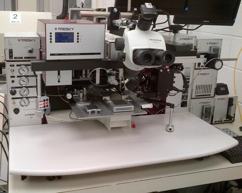
The Tresky T-3000-FC3-HF flip chip bonder can dispense solder pastes and epoxies, place solder preforms, and bond various types of devices onto semiconductor packages, submounts, and whole wafers. The system is equipped with a camera-based vision system to precisely align the parts that will be bonded together.
Specifications/Capabilities
- Eutectic bonding.
- Ultrasonic bonding.
- Thermo-compression bonding.
- Epoxy bonding.
- X and Y motion range: 200 mm.
- Die positioning accuracy: 1 µm.
- Die spindle rotation range: 2p (360 °).
- Side-view camera for direct observation of bonding process.
- Bond force: 50 grams to 400 grams.
- Tool heat up to 400 °C.
- Substrate heat up to 400 °C.
- Inert gas blanket.
Usage Information
Supported Sample Sizes
- Maximum wafer diameter: 150 mm (6 in).
- Small pieces supported: Yes.
- Maximum thickness: 40 mm.
Typical Applications
- Chip attachment to semiconductor, opto-electronic, microwave, and other packages.
Created June 19, 2014, Updated March 4, 2025