
Official websites use .gov
A .gov website belongs to an official government organization in the United States.
Secure .gov websites use HTTPS
A lock (
) or https:// means you’ve safely connected to the .gov website. Share sensitive information only on official, secure websites.
Guided Wave Electromagnetics Group
The Guided Wave Electromagnetics Group conducts theoretical, computational, and experimental research to deliver the basic metrology, special measurement techniques, and measurement standards needed for advancing both conventional and microcircuit guided-wave technologies, including coaxial, waveguide, and on-wafer geometries, at frequencies from 100 kilohertz (kHz) through 500 gigahertz (GHz).
Overview
The Guided Wave Electromagnetics Group provides fundamental electromagnetics research, including measurements, modeling, and theory, to support advanced wireless communications and other key national priorities in electromagnetics at radio frequency (RF), microwave, and millimeter-wave (mmWave) frequencies. Research is focused on traceable measurements of fundamental microwave quantities such as power and impedance; advanced guided-wave measurements and standards for integrated-circuit environments; fundamental material properties and modeling at RF, microwave, and mm-wave frequencies; and the electromagnetic response of soft materials such as liquids, polymers, and composites.
These metrology tools form the fundamental building blocks needed for the accurate description of more complex systems, including modern wireless communications systems at frequencies up to 100 GHz and beyond, advanced packages for heterogeneous integrated circuits, and the intermolecular electromagnetic environment of molecular solutions and inhomogeneous composites. Accurate measurements and standards at these frequencies support the continued rapid development of new application spaces in wireless communications, microelectronics and advanced packaging technologies, and electromagnetic sensing. Significant outcomes include traceable measurements and standards that underpin cutting edge research in multidisciplinary fields including electrical engineering, materials science and device physics. Results are disseminated to stakeholders directly through measurement services in power and scattering parameters, through the development of standard reference materials, via verification and validation programs with other government agencies, and with academic partners in publication of cutting-edge measurement science techniques.
Projects within the Guided Wave Electromagnetics Group complement other work at the National Institute of Standards and Technology (NIST) and within the RF Technology Division to provide the broad range of measurements and standards to accelerate U.S. research and development in critical and emerging technologies such as Integrated Communications and Advanced Engineered Materials. Work also supports overarching NIST initiatives including the CHIPS Metrology Program, the NIST on a CHIP initiative, and several Innovations in Measurement Science projects.
The identification of efficient strategies for the dissemination of fundamental measurement quantities, including standards and measurement data, analysis approaches, and modeling, is also a key focus of the Guided Wave Electromagnetics Group. Measurements of traceable fundamental quantities such as microwave power and scattering parameters are delivered directly to customers including U.S. companies and Department of Defense Primary Standards Laboratories through established measurement services. Special tests are another delivery method for NIST measurements, along with dedicated projects delivering needed standards and measurements for verification and validation to other government agencies. Measurement data for materials is delivered to an emerging customer base of U.S. companies through standard reference materials and on-chip standards. Research projects impacting U.S. semiconductor manufacturers are facilitated through research agreements in support of the NIST CHIPS Metrology Program.
For most research efforts, effective partnerships have been established with leading U.S. academic institutions to help broaden the impact of NIST measurements. Active participation in the NIST Professional Research Experience Program provides critical workforce development opportunities to help satisfy a growing future U.S. need for a highly trained technical workforce.
MAJOR ACTIVITIES
Traceable Impendance
Fundamental metrology in communications requires the ability to unambiguously determine the impedance of a reference environment and to provide linear transformations of measurements to measurement reference planes of interest. This is accomplished for multiple conducted systems through a series of physical standards, which are used to determine a 50-ohm reference impedance, with rigorous uncertainty analysis, and disseminated through a quality-managed comparative measurement process.
NIST serves as the National Metrology Institute (NMI) for the United States. As an NMI, NIST performs Scattering-parameter calibration services that provide the technical basis for international trade, commerce, and regulatory affairs.
Microwave Power Metrology
Every commercial microwave power sensor in the United States requires calibration. These sensors share near-ubiquitous traceability to the NIST Traceable Power project. As a result, NIST plays a key role in the communications industry, where power is king. Everything from handset battery life to wireless interference to eNodeB energy consumption depends on detailed measurements of power levels, including measurements at the integrated-circuit, connectorized-reference-plane, and over-the-air levels. To support the broad range of needs in the communications industry, NIST must focus its efforts on the highest-tier, highest-impact measurements while building a set of tools that can be readily deployed to industry.
Microwave Materials and On-Chip Standards
Finite-element and multi-physics simulations are ubiquitous in the design and development of devices for current and future generation wireless communications, such as integrated multi-band filters, switches, interconnects, duplexers, circulators, etc. The accuracy of models for wireless communications components depends primarily on the accuracy of the input material parameters, which can be difficult to evaluate over a broad range of frequencies, particularly for materials that display inhomogeneous, anisotropic, and/or nonlinear properties. Metrology focused on the accurate evaluation of microwave material properties beyond the linear, isotropic, and homogeneous limits will enable new approaches in microwave component design for interference mitigation, higher energy efficiency, higher spectral efficiency, and higher levels of integration in wireless communications. This is accomplished primarily through the detailed comparisons of computational models with accurate, broadband measurements of custom-fabricated planar test structures.
Metrology for Communications Electronics
A critical need for accurate measurements of microelectronic circuits exists at frequencies from 1 GHz to 1 terahertz (THz) to support emerging wireless communications and advanced microelectronics and packaging technologies. To enable accurate measurements at the circuit- and sub-circuit level, NIST leads efforts to develop wideband calibration and de-embedding tools, as well as modeling efforts to describe the propagation of signals at these small length scales and high frequencies. As circuit and package sizes decrease, nonlinear effects become more and more common, and NIST nonlinear measurements and calibration techniques provide new tools to assess the impacts of these effects. These measurements are applied to increase the security, reliability, and resiliency of modern chip-scale circuits and devices.
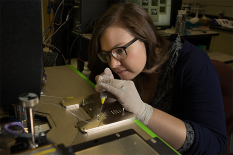
Electromagnetics of Soft Materials
Soft materials, including polymers, fluids, and gels, as well as composite materials, have become key components in many emerging electronics applications, including power electronics and packaging, as well as radio-frequency-based applications such as flexible electronics, micro-electromechanical systems (MEMS), lab-on-a-chip platforms, liquid-cooled circuits, and microwave reactors. These applications represent rapidly growing market segments in both microelectronics and advanced communications, where validated material characterization approaches and standards are notably lacking.
Publications
Awards
Contacts
Group Leader
-
(303) 497-7900