After powering five decades of innovation, Moore’s Law is faltering. Here’s how the National Institute of Standards and Technology (NIST) is helping the industry move forward.
As transistor scaling reaches its physical limits, industries are now faced with several key challenges in packaging, from mechanical stress and distortion to electrical interference, environmental effects, and failure mechanisms.
Polymer-based packaging materials, once viewed as little more than a means to glue or encase the chip, have now emerged as important factors for reliability, performance, and cost. The industry increasingly recognizes the need for reliable methods to characterize and predict material behavior, standardized benchmarks to correlate polymer performance, and effective solutions to mitigate costly failures.
A new perspective article from NIST and collaborators* highlights this critical but often underrated piece of the semiconductor revolution: the polymer-based “soft” materials that hold advanced chips together.
Polymers—such as epoxies, silicones, and polyimides—encapsulate chips, connect them to circuit boards, and keep them running reliably. As industry shifts toward 3D heterogeneous integration, where multiple chips are stacked or linked in three dimensions, the demands on these materials are rapidly escalating.
The challenge of soft materials
Unlike metals or ceramics, polymers are time- and temperature-sensitive, absorbing moisture and changing shape under stress. These behaviors can cause chips to warp, signals to degrade, or connections to fail over years of operation. Traditional materials, many of which have not changed much in decades, now face new performance demands in applications like 5G/6G communications, artificial intelligence, and high-performance computing.
“Polymer science is fascinating to polymer scientists, but that fundamental knowledge is often lacking in the packaging world,” said Ran Tao, lead author of the paper. “Those fundamentals are valuable and can help guide industrial decision-making.”

A metrology-first approach
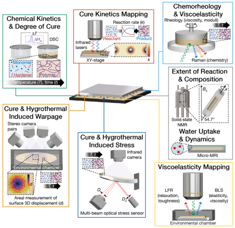
The article highlights new measurement techniques being developed at NIST, from advanced rheology and spectroscopy to stress measurements. These tools help track how polymers cure, shrink, and deform during manufacturing—factors that directly impact device reliability.
As industry pushes toward digital twins and predictive design, accurate measurements become indispensable. “Modeling without metrology is imagination,” stated co-author William Chen, Chair of the Institute of Electrical and Electronics Engineers (IEEE)’s Heterogenous Integration Roadmap for semiconductors.
NIST is also pioneering research-grade test materials (RGTMs): open, nonproprietary polymer systems that serve as benchmarks. Unlike commercial “black box” materials, RGTMs allow researchers across industry, academia, and government to compare results, improve reproducibility, and feed reliable data into computer models.
“RGTMs are key,” said Christopher Soles, NIST materials scientist and co-project leader. “By providing shared, transparent materials, we can accelerate innovation across the entire ecosystem.”
Building resilience and collaboration
This perspective grew out of a NIST-organized workshop at the 2024 Electronics Packaging Symposium, where experts from industry, universities, and government labs agreed on key priorities. These include rebuilding U.S.-based supply chains for packaging materials, creating shared databases of material properties, and advancing measurement standards.
For Amanda Forster, also a NIST researcher and co-lead, the effort ties directly to the institute’s broader mission: “NIST’s role and mission to advance measurement science and support U.S. industry has never changed.”
With some new packaging materials taking 10 to 25 years to reach production, the authors stress that early, collaborative work is essential. By bridging the gap between polymer science and semiconductor engineering, the U.S. can accelerate innovation while strengthening supply chain resilience.
Reference:
*R. Tao et al., “Material Needs and Measurement Challenges for Advanced Semiconductor Packaging: Understanding the Soft Side of Science,” IEEE Transactions on Components, Packaging and Manufacturing Technology, 2025. DOI: 10.1109/TCPMT.2025.3603484

