
Official websites use .gov
A .gov website belongs to an official government organization in the United States.
Secure .gov websites use HTTPS
A lock (
) or https:// means you’ve safely connected to the .gov website. Share sensitive information only on official, secure websites.
NanoFab Tool: Plasma Therm Corial Deep Silicon Etcher
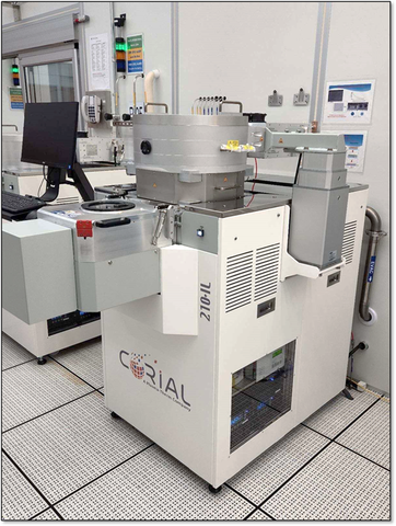
The Plasma-Therm deep silicon etcher is an inductively coupled plasma (ICP) reactive ion etching system used for etching deep features in silicon. The tool uses a fast switching Bosch process that produces vertical sidewall profiles. The manual load system can accommodate substrates ranging from 200 mm diameter wafers down to small pieces.
Specifications/Capabilities
- Inductively coupled plasma (ICP) power source: up to 2000 W.
- Radio Frequency (RF) power source: up to 600 W.
- Process gases: Ar, O2, He, N2, CHF3, C4F8 and SF6
- Anisotropic deep etching of silicon.
Usage Information
Supported Sample Sizes
- Maximum wafer diameter: 200 mm.
- Small pieces supported: Yes.
Typical Applications
- Microelectromechanical systems (MEMS).
- Nanoelectromechanical systems (NEMS).
- Through silicon vias (TSV) for three dimensional integration.
- Microfluidic devices.
Created December 18, 2024, Updated March 4, 2025