Summary
With the rise of artificial intelligence and its insatiable demand for low-energy, high performance computing, research is accelerating into novel nanodevices that perform new functions like large scale vector matrix multiplication or synaptic weighting and neuronal response. To evaluate the performance of these functions, experimental devices must be integrated with complementary metal oxide semiconductor (CMOS) electronics. We are enabling this research by creating a suite of testbeds with the goal of making it possible for a wide variety of researchers to easily explore new devices, circuit architectures and functionalities.
Description

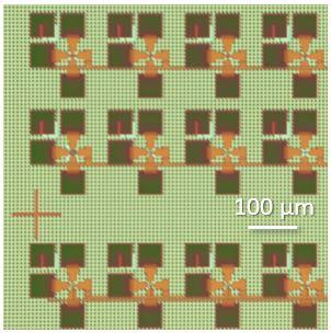
Small array of transistors designed for single device integration.
The increasingly complex device requirements for next-generation computing architectures such as neuromorphic computing or nanoelectronic machine learning accelerators present challenges for researchers across the spectrum of institutions, from small businesses and universities to government laboratories and large corporations. Many applications in artificial intelligence require extremely large numbers of devices and are sensitive to device parameter variations. Measuring large numbers of devices, experimentally verifying device-algorithm interactions, and rapidly generating the immense quantities of data needed to study the field’s biggest challenges present some of the most significant impediments to progress. Other problems, such as the impact of device parasitics, create difficulties for performing in situ experiments on emerging devices. To tackle these issues, we are developing flexible, easy-to-use CMOS measurement platforms that are tailored for integration with novel devices via back-end-of-line processes in local fabrication facilities. These platforms are enabling us and our collaborators to create new families of nanodevice measurements and foster a rapid expansion of research in new forms of integrated electronics for advanced information processing.
To build our platforms for direct integration with sophisticated active elements, we exploit the existing semiconductor supply chain to acquire wafer scale CMOS technology in fabrication-friendly form factors (including 200mm/100/75 mm wafer scales and small die) to directly integrate with novel devices. Our acquired CMOS platforms, designed by NIST, are fully planarized with vias accessible to the substrate transistors. In addition, we include alignment marks compatible with contact, stepper, and e-beam lithography so researchers can easily integrate CMOS into their nanofabrication development.

Individual Device Arrays
Because many emerging nanodevices operate at extremely high speed and are very sensitive to transients and parasitic effects, we are creating individual NMOS and PMOS transistors for direct integration with single devices. With contact pads accessible to conventional laboratory wire bonding, these individual transistors can be cointegrated with nanodevices and staged in measurement platforms such as scanning electron microscopy, transmission electron microscopy, or atomic force microscopy among many other capabilities. The directly integrated transistor completely eliminates the parasitic effects of wire and contact capacitance, which can easily destroy devices, and improves the measurement stability, accuracy, and reproducibility. These platforms are making possible a whole new range of experiments that elucidate the underlying physics of device behavior.
Large Scale Arrays
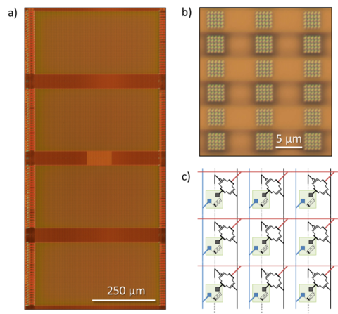
While small arrays satisfy the needs of individual device characterization experiments, we are also building large-array test beds for statistical evaluation of large numbers of nanoscale devices and array-level-controlled experiments. For example, we have created a “2-transistor, one resistor” (2T-1R) array that can operate in either an active mode, with individual transistors acting as selector devices, or in a passive mode, where the transistors are fully turned on to simulate the operation of a passive crossbar array. The impact of line resistance is minimized by implementing all array level routing in the CMOS layers, eliminating the need for post fabrication planarization and patterning of low resistance transmission lines. Using hardware timed measurements, devices can be measured at a speed of 20,000 devices per second, making it seamlessly easy to generate the large datasets needed to model the operation and training of large-scale hardware neural networks.
Device-Algorithm Interaction
To fully realize their measurement capability, single-device and large-scale CMOS arrays can also be co-integrated into commercial off the shelf measurement hardware or custom printed circuit boards with field programmable gate array control systems. These control systems can directly implement model hardware neural networks and directly test device-algorithm interactions. This capability is used to benchmark the performance of certain classes of nanodevices under different learning rules and operational modes. We use the data from these experiments to develop additional, alternative algorithms which are better suited to the nanodevice environment or device non-idealities present within a particular family of nanodevices.

