
Official websites use .gov
A .gov website belongs to an official government organization in the United States.
Secure .gov websites use HTTPS
A lock (
) or https:// means you’ve safely connected to the .gov website. Share sensitive information only on official, secure websites.
NanoFab Tool: Zeiss Ultra 60 Field Emission Scanning Electron Microscope
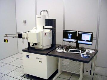
The Zeiss Ultra 60 Field Emission Scanning Electron Microscope (FE-SEM) is a high resolution FE-SEM which provides nanoscale imaging and compositional analysis on substrates ranging from 150 mm diameter wafers down to small pieces. It has superb resolution and image quality at high and low accelerating voltages. The Ultra 60 has a high efficiency in-lens secondary detector for high contrast topographic imaging. It also has an energy selective back scatter detector and a solid state retractable backscatter detector for compositional contrast imaging at both high and low voltages. The Ultra 60 is equipped with an energy dispersive x-ray spectroscopy (XEDS) analysis system for elemental analysis.
Specifications/Capabilities
- Digital system with full function computer control.
- Resolution: 1.0 nm at 15 kV; 1.6 nm at 1 kV.
- Magnification: 12 times to 1,000,000 times.
- High efficiency in lens secondary detector for high contrast imaging.
- Energy selective backscattered electron detector for compositional contrast imaging at low voltages.
- Four quadrant, solid state backscatter detector for compositional contrast imaging and topographical imaging at high accelerating voltages.
- Motorized stage with travel in 6 axes.
- Integrated 150 mm airlock for fast sample changes.
- Oxford 80 mm2 X-Max silicon drift XEDS detector for elemental composition and mapping.
Usage Information
Supported Sample Sizes
- Maximum wafer diameter: 150 mm (6 in).
- Small pieces supported: Yes.
Typical Applications
- Measurement and inspection of nanometer scale structures.
- Determination of the elemental composition of specific sites on a sample.
- Collection of elemental maps and line scans from specific areas of a sample.