
Official websites use .gov
A .gov website belongs to an official government organization in the United States.
Secure .gov websites use HTTPS
A lock (
) or https:// means you’ve safely connected to the .gov website. Share sensitive information only on official, secure websites.
NanoFab Tool: Plasma-Therm Versaline High Density Plasma Enhanced Chemical Vapor Deposition (HD-PECVD)
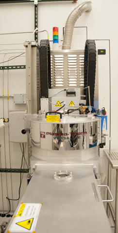
The Plasma-Therm Versaline high density plasma enhanced chemical vapor deposition (HD-PECVD) system uses an inductively coupled plasma to remotely ionize deposition molecules at high power away from the substrate. It then draws the ionized molecules to the substrate surface at low energy which reduces surface temperature while producing a high density film. This technology provides a low temperature alternative to furnace driven processes and conventional plasma enhanced chemical vapor deposition methods for the deposition of silicon dioxide, and silicon nitride. The HD-PECVD system produces high quality, pinhole-free films that are comparable to high temperature furnace deposited films. The system can accommodate substrates ranging from 100 mm diameter SEMI spec Silicon wafers down to small pieces.
Specifications/Capabilities
- Maximum radio frequency (RF) bias power: 600 W.
- Maximum inductively coupled plasma power (ICP): 2000 W.
- Maximum substrate temperature: 180 °C.
- Film thicknesses ranging from a few nanometers to several micrometers.
- Processes supported:
- Silicon dioxide.
- Silicon nitride.
- Silicon Oxynitride.
Usage Information
Supported Sample Sizes
- Maximum wafer diameter: 100 mm SEMI spec Silicon wafer.
- Small pieces supported: Yes.
- Maximum thickness: 1 mm.
Typical Applications
- Optical waveguides.
- Silicon gate devices.
- Solar cell fabrication.