
Official websites use .gov
A .gov website belongs to an official government organization in the United States.
Secure .gov websites use HTTPS
A lock (
) or https:// means you’ve safely connected to the .gov website. Share sensitive information only on official, secure websites.
NanoFab Tool: Denton Vacuum Discovery 550 Sputtering System B104 Right
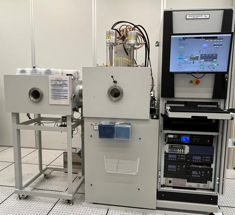
Denton Vacuum Discovery 550 Sputtering System B104 Right
The Denton Vacuum Discovery 550 sputtering system has two direct current (DC) and two radio frequency (RF) sputtering guns which bombard targets, causing atoms to be ejected in order to support a wide range of thin film deposition processes. Both DC guns are magnetically enhanced to allow for deposition of ferromagnetic materials. A computer controlled user interface enables unattended sequencing of multiple deposition layers. The system has a heated, rotating stage for superior stress control and uniformity on substrates ranging from 150 mm diameter wafers down to small pieces.
Specifications/Capabilities
- Turbo-pumped vacuum chamber has a base vacuum of 2.6 x 10⁻⁵ Pa (2 x 10⁻⁷ Torr).
- Rotating stage for high uniformity deposition of thin films.
- Stage temperature range: 25 °C to 350 °C.
- 600 W DC and RF power supplies.
- Two RF and two DC guns.
- Both DC guns are magnetically enhanced for ferromagnetic materials.
- Computer controlled interface enables unattended sequencing of multiple deposition layers.
- Co-sputtering capability from one RF and one DC gun.
- Argon bombardment can be used to remove native oxide from wafers.
- Oxygen and nitrogen available for reactive sputtering.
- List of available sputtering targets: Ag, Al, Al/Si(99/01), Al2024, Al2O3, AlN, Au, Co, Cr, Cr (reactive), Cu, Cu/Ni (55/45), Fe, Fe (reactive), Gd, Ge, ITO, Li3PO4, LiCoO2, Mo, Nb, Ni, Ni/Fe(81/19), Pd, Permalloy, Pt, Pyrex 7740, Si, Si(n), Si(p), Si3N4, SiC, SiO2, SiO2(Eu), SnO2, Ta, Ta2O5, Ti, Ti (reactive), TiO2, V, V2O5, W, W/Ti(90/10), WC, Yb2O3, Zr, ZrO2(Yb2O3)
Usage Information
Supported Sample Sizes
- Maximum wafer diameter: 150 mm (6 in).
- Small pieces supported: Yes.
Typical Applications
- Electrical contacts.
- Dry etch masks.
- Magnetic materials.
- Electrical isolation.