
Official websites use .gov
A .gov website belongs to an official government organization in the United States.
Secure .gov websites use HTTPS
A lock (
) or https:// means you’ve safely connected to the .gov website. Share sensitive information only on official, secure websites.
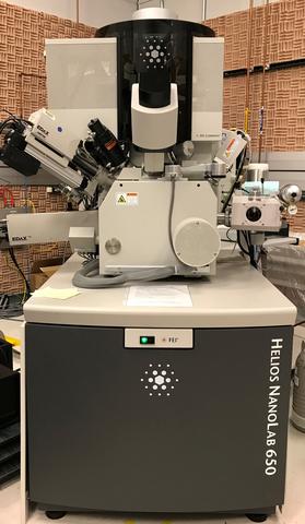
Focused Ion Beam Scanning Electron Microscope (Helios 660)
MML/MMSD (Div643) Helios 660 Focused Ion Beam Scanning Electron Microscope
The Helios 660 NanoLab (HNL660) is a Focused Ion Beam Scanning Electron Microscope equipped with spectroscopic detectors to allow elemental and phase measurements to be performed at high spatial resolution. The HNL660 operates between 1 keV and 30 keV electron beam energy and 2 kV and 30 kV ion beam accelerating voltage. The HNL660 has an Elstar thermal (Schottky) field emission electron source and a Tomahawk ion column using a Ga+ liquid metal ion source. It is used for a variety of applications such as 2D and 3D chemical imaging of organic and inorganic samples at room temperature and under cryogenic conditions, transmission electron microscopy and atom probe tomography specimen preparation, and automated hyperspectral x-ray microanalytical method development. The HNL660 is also equipped with retractable STEM detector, cryo stage, nano manipulator, multiple gas injection systems, two EDS detectors (windowed and windowless), and an EBSD system.
Specifications/Capabilities
* up to 30 keV electron beam energy
* up to 30 keV ion beam energy and 60 nA ion beam current
* 5-axis stage
* silicon drift detectors (30 mm^2)
* windowless silicon drift x-ray detector (100 mm^2)
* high resolution electron backscatter diffraction system
* cryo stage and sample preparation system
* nano-manipulator system for TEM sample prep
* scanning transmission electron microscopy detector
* Everhardt-Thornley detector, through-the-lens detector, in-column backscattered electron detectors, ICE detector
Scientific Opportunities/Applications
* nanofrabrication
* 2D & 3D phase, elemental, and morphological analysis
* 2D & 3D cryo analysis of organic and polymeric samples
* nanostructure and nanoparticle imaging and analysis
* TEM and APT specimen preparation
Usage Information
Access Information
Individual collaborative projects to address NIST measurement needs are possible when the work is consistent with the Materials Measurement Science Division mission space. Contact Keana Scott to discuss possible collaborations.