
Official websites use .gov
A .gov website belongs to an official government organization in the United States.
Secure .gov websites use HTTPS
A lock (
) or https:// means you’ve safely connected to the .gov website. Share sensitive information only on official, secure websites.

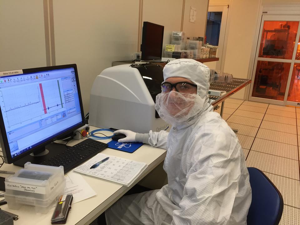
Shamir Maldonado-Rivera's internships at the NIST NanoFab led to her getting her dream job at NASA.
A Nanofabulous Experience: Internship at NIST’s NanoFab Provides Vital Training for Engineers and Technicians Entering the Semiconductor Workforce
Even before Shamir Maldonado-Rivera graduated from the University of Puerto Rico in 2019 with an applied physics degree, she had already picked out her dream job working with semiconductors.
The only problem was that she lacked the hands-on experience.
Her university studies hadn’t given Maldonado-Rivera the chance to work in a “clean room” — the ultra-dust-free environment necessary to fabricate and examine tiny electronic components on silicon chips and other semiconductor materials. Nor had she ever operated precision tools to etch microscopic circuits or used specialized software to identify and analyze fabrication errors made by the tools.
Maldonado-Rivera acquired those skills and more during a monthslong internship at the National Institute of Standards and Technology (NIST) NanoFab facility, which provides researchers with rapid access to state-of-the-art nanoscale measurement and fabrication tools and methods, along with technical expertise.
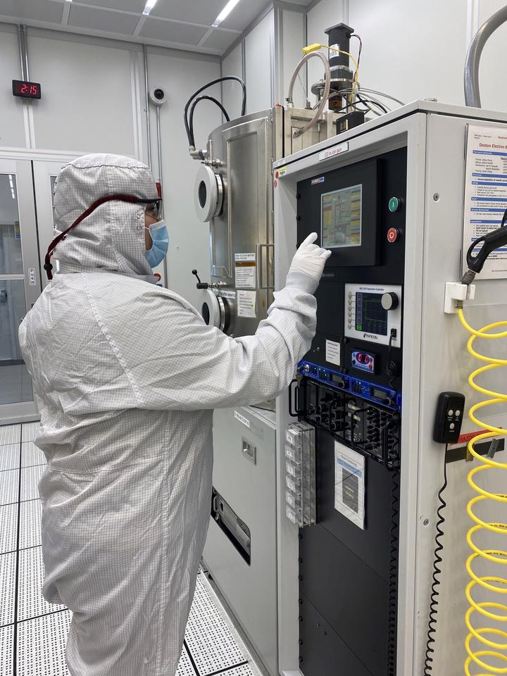
Shamir Maldonado-Rivera got hands-on clean-room experience during her internships at NIST NanoFab.
NanoFab internships are one of the many ways that NIST and the Department of Commerce are helping to ensure American preeminence in semiconductors. Since its inception in 2014, 37 budding engineers and technicians in the semiconductor industry have completed the NIST program, which provides critical hands-on knowledge for tomorrow’s semiconductor-industry workforce at NIST and throughout the U.S.
At the NanoFab, Maldonado-Rivera used highly focused beams of ions and electrons to imprint, or incise, silicon wafers with patterns a mere 20 nanometers — about 20 times the thickness of a strand of human DNA — in depth.
Engineers guided her as she experimented with photolithography, an imprinting technique in which light shines through a photomask — a thin, opaque film with sections cut out in an intricate design — onto wafers coated with a light-sensitive medium. While mastering that technique, she became familiar with the stepper (short for step-and-repeat camera), a device similar to a slide projector that rapidly imprints millions of microscopic circuit elements on a succession of wafers.
‘There Was So Much More I Wanted to Learn’
Maldonado-Rivera had intended to return to Puerto Rico after her three-month internship ended in December 2019, but there were still many tools in the NanoFab that she hadn’t had a chance to operate.
“There was so much more I wanted to learn,” she said.
Encouraged by her mentor, NanoFab assistant manager Jessie Zhang, she applied for and was granted a second internship.
During that time, she was tasked with improving the reliability of an etching tool that uses a beam of ionized gas to create intricate patterns on silicon chips. The tool’s performance was inconsistent: It did not always cut grooves that were perfectly perpendicular to the surface of a chip.
Analyzing electron micrographs of the grooves after varying several properties of the ion beam, Maldonado-Rivera found that reducing the pressure and flow, along with shortening the etching procedure, enabled the tool to more reliably incise the grooves. In reporting the results of her study, Maldonado-Rivera learned how to write a technical report clearly and concisely.
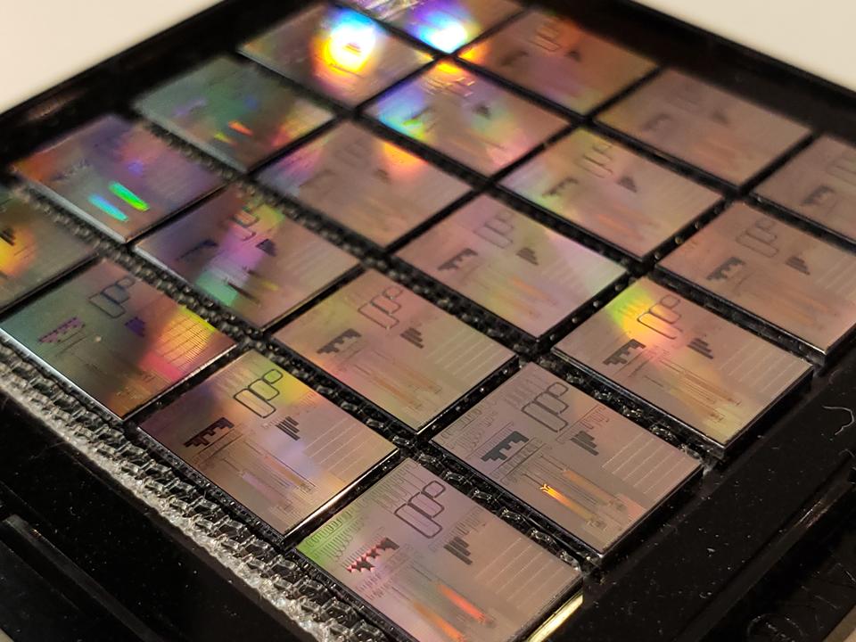
Photonics chips ready for assembly and packaging.
In November 2019, it was time to put her newfound skills to work. She applied several times to Northrop Grumman, the aerospace and defense technology company, after spotting a job opening that listed photolithography as one of the required skills. After not hearing back for six months, she assumed the company wasn’t interested. But in June 2020, Northrop Grumman contacted her, and a month later she began work as a process engineer at the firm’s Baltimore location.
When the company gave her a choice of instruments to operate, she chose the stepper. Unlike the tool at NIST, the Northrop Grumman stepper was automated and could fabricate 16 batches of 16 to 20 silicon chips in a single day. She loved the fast pace and the challenge of working with a tool that was highly sensitive to changes in vibration and humidity and to stray particles from the silicon chips. Soon, other team members were consulting her about chip fabrication.
Maldonado-Rivera’s career continued to flourish, and by September 2021 she was considering transferring to a different branch of the company to learn new skills. That’s when she got the call she had long hoped for.
The call was from NASA.
‘You Have the Skills’
Early in her internship, Maldonado-Rivera had visited NASA’s Glenn Research Center in Cleveland, where a manager who was also an alumnus from Maldonado-Rivera’s university had shown her around and kept a copy of her resume. Maldonado-Rivera had always wanted to be a NASA engineer and she hoped that sometime in the future, maybe in 10 years, she might land a job there.
Now the agency wanted to interview her for an engineering position that had just opened. When she saw the pay grade for the job, Maldonado-Rivera thought that the position was beyond her reach and that only someone with a Ph.D. would be hired. In the days leading up to the interview, she doubted herself. Was she really ready for this?
A co-worker assured her she was. “You have the skills,” her colleague told her. “You are enough.”
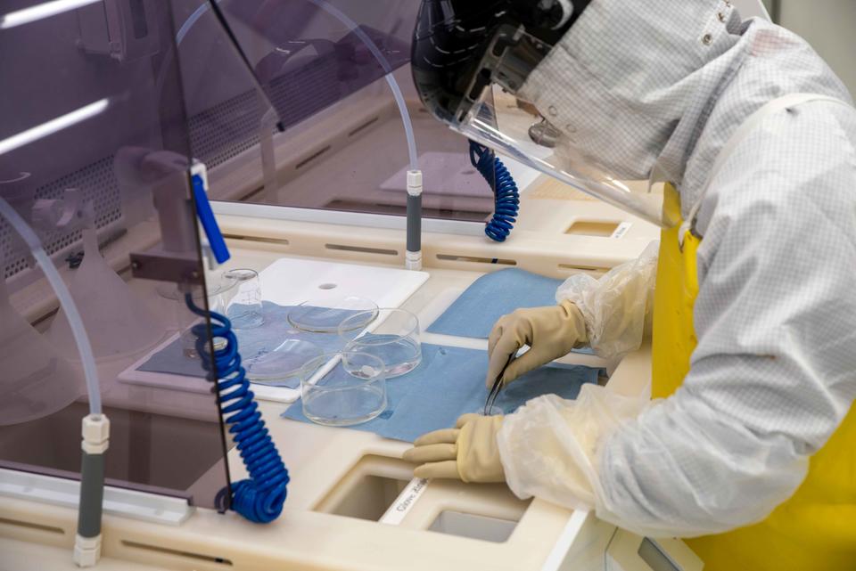
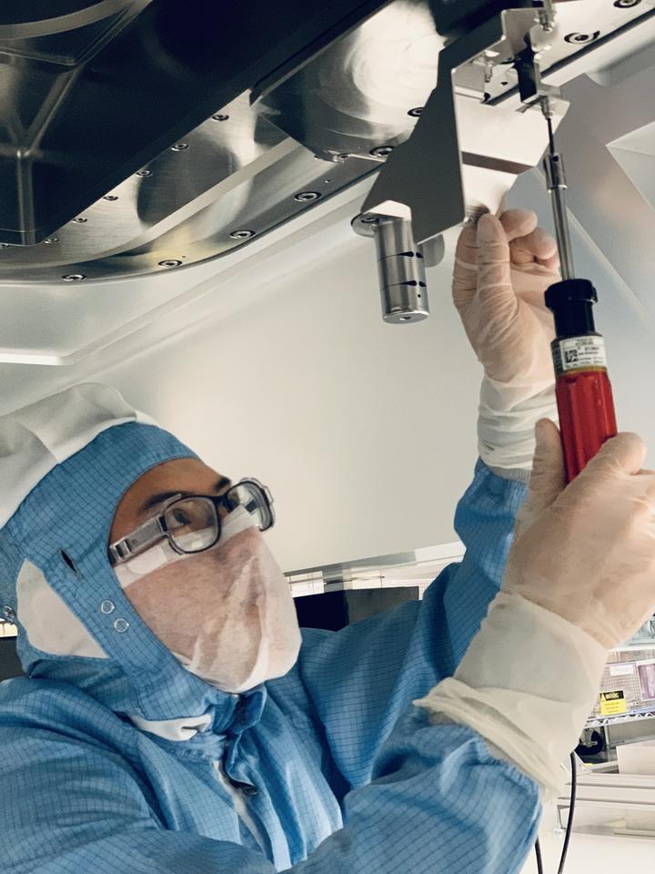
It takes a lot of chemistry to make a computer chip. Here a NanoFab user is working with acids while wearing the proper personal protective equipment (PPE).
The interview went well, but for weeks Maldonado-Rivera did not hear from the space agency. She called to inquire and was told to wait. On a workday in October 2021, Maldonado-Rivera was away from her desk at Northrop Grumman for a few minutes. When she got back, she noticed a call on her cellphone from NASA. “OMG, OMG,” she told herself as she quickly returned the call. But the person at NASA had already left for the day.
She would have to wait another 24 hours to get the news: She had landed her dream job.
On Oct. 25, 2021, Maldonado-Rivera got her NASA badge and laptop and took her oath of office. She was really there. She had made it.
Hired as a systems processing engineer, Maldonado-Rivera began work fabricating and helping to design tiny electrical devices for a spacecraft that NASA hopes will begin orbiting Venus late in the next decade. Recently promoted, she is now supervising other scientists in her group, who often consult her on designs.
“If it wasn’t for the NanoFab and my mentor, Jessie Zhang, I wouldn’t be here at NASA right now,” she said.
The NIST NanoFab internship is co-sponsored by the Northeast Advanced Technological Education Center (NEATEC) through a grant from the National Science Foundation. Hosted by the State University of New York Polytechnic Institute, NEATEC advertises the program nationwide and also selects the three most promising candidates among the applicants.
‘I Want to Motivate More People’
Maldonado-Rivera has been doing some mentoring of her own. Staying in touch with students and faculty members from her university, she told them how much the NanoFab internship had helped her. That’s a key reason that Giovanna M. Castejón-Cruz, who graduated from the University of Puerto Rico in 2021, applied.
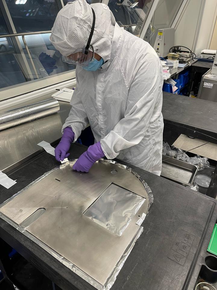
Castejón-Cruz began her internship in January 2022. During her four months at the NanoFab, she learned how to operate and maintain several instruments, including a sputtering tool. That device employs an energetic beam of ions to remove, or sputter, atoms from a target material such as gold or chromium. Inside a vacuum chamber, the sputtered atoms are then deposited onto a silicon chip, forming an ultrathin coating.
Using a direct-write laser, Castejón-Cruz inscribed chips with tiny, three-dimensional structures. She also conducted experiments in photolithography.
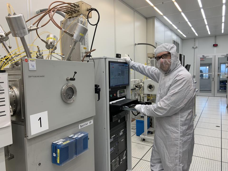
Giovanna Castejón-Cruz learned how to operate and maintain several instruments during her four months at the NanoFab.
Toward the end of her internship, Northrop Grumman contacted Castejón-Cruz about a job in fabricating microelectronics. Zhang guided Castejón-Cruz through the interview process, and Maldonado-Rivera sent encouraging emails.
Castejón-Cruz knew that the internship had given her the foundation she needed to qualify for the position.
When Northrop Grumman made her a job offer in April, the first people Castejón-Cruz called were her family. Then she made a second call, sharing the exciting news with Maldonado-Rivera.
Like Maldonado-Rivera, Castejón-Cruz has become a strong advocate for the internship. “I’m sharing my experience at NIST's NanoFab because I want to motivate more people from minority groups to feel encouraged and know that they can also participate in opportunities such as this one to gain a foothold in the semiconductor industry,” she said.
More Success Stories
Castejón-Cruz and Maldonado-Rivera are far from the only success stories. A host of other students who completed the NanoFab internship immediately landed jobs in the semiconductor industry and continue to thrive there.
In 2016, Alex Galli graduated from the University of Kansas with a keen interest in nanotechnology but little training in the field. During his NanoFab internship, he operated an electron microscope and vapor deposition tools and became familiar with quality control software.
Always looking toward the future, Galli had applied for a job at Northrop Grumman even before he began his internship. The interview took place while he was at the NanoFab.
"My training at the NanoFab definitely set me apart from everyone else," Galli said.
Alex Galli learned how to use quality control software during his internship at the NanoFab.
He finished the internship on a Friday and joined Northrop Grumman at its Linthicum, Maryland, location, the following Monday. Initially working in the nanotech clean room, Galli is now a senior principal metrology process engineer at the company.
When Patricio Xavier Flores Granda began his internship at the NanoFab in January 2018, he had never donned a bunny suit (the coveralls required in the clean room) or worked with the precision tools that fabricate nanostructures. Working closely with several NanoFab process engineers, Flores Granda quickly learned how to maintain and prep instruments for researchers from academia, industry and NIST. He also became adept at using software to track the reliability of machines designed to deposit precisely calibrated, ultrathin coatings of metals and polymers on silicon wafers.
Soon he was assisting other interns as they learned how to change out the solid targets that are vaporized and then condensed on silicon wafers to form thin films.
At the clean room at ASML, former NanoFab intern Patricio Xavier Flores Granda manufactures the top module of an extreme-ultraviolet instrument that imprints silicon wafers with the tiniest of features, enabling mass production of some of the world’s most advanced microchips.
During a job interview at ASML, a manufacturer of advanced semiconductor processing equipment based in Wilton, Connecticut, Flores Granda left nothing to chance. He not only recounted his experience in the NanoFab but gave a PowerPoint presentation about his internship. To no one’s surprise, ASML hired him as a production technician.
In 2020, the company promoted him to systems test engineer for a project that uses extreme ultraviolet light to imprint microchips with structures a mere 30 hydrogen atoms in depth. He integrates and tests new hardware and software for the extreme-ultraviolet instruments. With a master’s degree in mechanical engineering already under his belt, Flores Granda is now pursuing a second master’s in systems engineering.
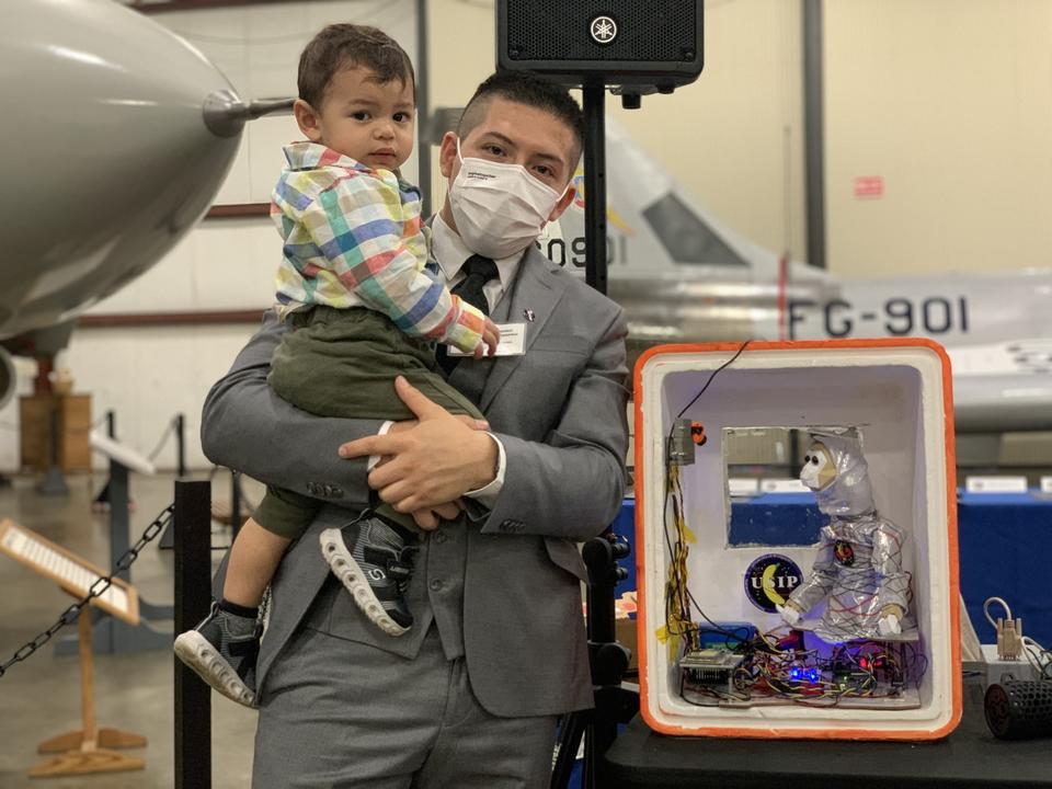
Patricio Xavier Flores Granda, now continuing his graduate studies, poses with his son at a 2021 NASA consortium at the New England Air Museum, where he presented his work related to a high-altitude NASA balloon project.
‘A Career I Can Be Proud Of’
Among the interns that Flores Granda had assisted at the NanoFab was Evan Cooper. Switching to a technical career at age 37, Cooper had recently earned an associate applied science degree in nanotechnology at Erie Community College in Buffalo, New York, with a 3.99 GPA.
“Something about going back to school after eight years and knowing you’re going to pay for your schooling out of your own pocket made me want to sit in the front row and learn everything I could,” Cooper said.
By the time he began the first of two internships at the NanoFab in July 2018, he had already worked as a technician in the college’s newly built clean room.
Still, he had plenty to learn. When a researcher accidentally loaded a cassette of microchips upside down in a deposition tool, an engineering technician in the NanoFab showed Cooper how to painstakingly trace and resolve the cascade of problems the error had caused.
“The training showed me how to really approach a problem slowly and eliminate possible sources of error one at a time until I find the culprit,” Cooper said. “There is no better feeling than when you solve a problem that allows users to return to work on a project that might someday lead humanity to travel from one planet to another or help us evolve into a wiser and better species.”
Former intern Evan Cooper, shown here at the NIST NanoFab, now travels around the country and the world installing instruments.
Cooper also gained new respect for both the extraordinary properties and fragility of semiconductor materials. It amazed him to realize that a speck of dust sitting in the wrong place on a semiconductor device, such as those in the cellphones we take for granted, could cause the entire device to fail. And that salt or sodium traveling freely through a semiconductor can severely damage its electrical properties.
Those lessons, he said, were enormously helpful when Heidelberg Instruments hired him as a field services engineer in the fall of 2019, just after his second internship at the NanoFab. Traveling to different sites in the U.S. and sometimes overseas, Cooper now operates million-dollar lithography tools and installs instruments so big that it takes more than a week just to assemble all the electrical cables and gas lines.
“I am so lucky they took a chance on me at the NanoFab because it gave me a career I can be proud of,” Cooper said.
“We need to attract more people in the U.S. into the nanotechnology and semiconductor industries,” he added, “and the NIST internship is one highly successful way to do that.”