
Official websites use .gov
A .gov website belongs to an official government organization in the United States.
Secure .gov websites use HTTPS
A lock (
) or https:// means you’ve safely connected to the .gov website. Share sensitive information only on official, secure websites.
Enabling Nanotechnology from Discovery to Manufacture
Challenge
With production using nanoscale components and processes soon expected to become a dominant factor, the United States faces dramatic changes in manufacturing in the 21st century. The promise of U.S. investment and innovation in nanotechnology can be realized only if the necessary infrastructure of measurement methods and standards is available to produce superior nanotechnology products.
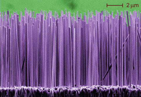
Products built from nanoscale components—a thousand times thinner than a human hair—require entirely new ways to accurately quantify their properties and determine their sizes, shapes, and chemical composition.
Proposed NIST Program
In FY 2007, NIST began a major initiative to address the measurement barriers hindering rapid development of nanotechnologies. A new NIST Center for Nanoscale Science and Technology (CNST) has been established that combines both research and a state-of-the-art nanofabrication and nanometrology user facility.
While a complementary NIST initiative will provide important groundwork in measuring environmental, health, and safety (EHS) risks of nanotechnology, this research initiative will build on recent NIST advances in developing nanoscale science and technology by:
- devising ways to measure strength, stress, strain, optical, and electronic properties of nanostructures to improve processes and understanding of failure mechanisms;
- creating three-dimensional, high-resolution imaging methods that reveal details of structure, chemical composition, and manufacturing defects and allow researchers to view nanostructures as they interact with their environment;
- simulating nanoscale phenomena with computer models to allow economical development of production methods for complex nanodevices; and
- pushing existing computer technology to its ultimate limit by developing measurements and standards that support "ultimate CMOS," or the development of current transistor technology to its technological limit.
Expected Impacts
NIST work in this area should help to:
- enhance the global competitiveness of U.S. manufacturers whose products incorporate nanotechnology;
- accelerate private-sector commercialization of new products and innovations such as high-strength, high-toughness materials for greater auto fuel efficiency and personal protection, as well as drug delivery systems with nanoscale components;
- enable more compact, powerful, and innovative products made with nanotechnology-enhanced electronic chips that are smaller, faster, and more efficient; and
- produce increased yield, productivity, and reliability in the manufacture of nanostructures and devices for the electronics, sensor, information storage, and communications industries.