
Official websites use .gov
A .gov website belongs to an official government organization in the United States.
Secure .gov websites use HTTPS
A lock (
) or https:// means you’ve safely connected to the .gov website. Share sensitive information only on official, secure websites.
Ultra-fast Electrical Characterization of Nanoscale Devices in Extreme Environments
Summary
Advanced nanoscale devices are expected to support operation frequencies that reach into the GHz range and beyond. These same advanced nanoscale devices are also asked to operate in the harshest of temperature swings which span from cryogenic temperatures to several hundred degrees above room temperatures. These remarkably disparate situations evoke an array of more exotic device physics which govern operation. More importantly, these device physics are largely absent in the standard (room temperature, DC or quasi-DC) electrical characterizations which are often employed to assess the worthiness of advanced nanoscale devices. The aim of this project is fill in this knowledge gap by developing the measurement infrastructure to characterize the most novel device structures at extreme temperatures and extreme frequencies. This infrastructure includes wafer-level device and circuit electrical characterizations which capture device responses in the 10’s of picosecond time scales at temperatures which range from 4 K to more than 500 K. This measurement aptitude facilitates efforts to tease out the dominant nanoscale device physics in the most exotic transistor and memory devices. In addition, the low temperature characterization provides a library of device physics necessary to design the ancillary cryogenic circuits needed in a variety of quantum information science experiments.
Description
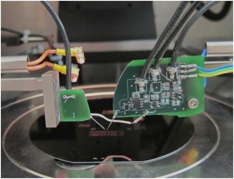
Custom ultra-fast electrical probes for wafer level characterization of advanced device transient operation
The ultra-fast characterization of advanced nanoscale devices is largely accomplished through a variety of custom impedance matched wafer probes, custom fast amplifier circuits, and a variety of fast electrical excitation sources. These excitation sources are commercial communications instruments which have been modified to be more suitable for individual device characterizations. In most cases, the custom wafer probes are designed such that more cumbersome high frequency device layouts (ground-signal-ground) are not necessary. Relaxation of this requirement allows for examinations of the dominant device physics in the most bleeding edge devices which are still in development and/or exotic device architectures which are still in their infancy. This approach has also proven quite useful in fast characterizations of novel non-volatile memories which may also have applications in the neuromorphic design space. Unsurprisingly, these characterizations revealed a variety of device physics which were previously ignored and proved dominant in circuit implementations.
The ultrafast electrical characterization competency can also be translated to measurements which occur at temperatures which deviate widely from room temperature. Similarly, the measurement infrastructure involves heavy modification to the wafer probes and designs of a cryogenic wafer probe station. This effort is undertaken to uncover the low-temperature device physics which are required to design and fabricate high frequency silicon circuits which operate at cryogenic temperatures. These in-situ circuits have applications which span high frequency current amplification to the generation of microwave pulse sequences. The applications of such circuits aid efforts in the quantum information science and quantum-adjacent research thrusts which permeate NIST.