
Official websites use .gov
A .gov website belongs to an official government organization in the United States.
Secure .gov websites use HTTPS
A lock (
) or https:// means you’ve safely connected to the .gov website. Share sensitive information only on official, secure websites.
Three-Dimensional Nanometer Metrology
Summary
We use physics theories to understand and simulate the interaction of electrons, light, and mechanical probes with nanometer-scale structures, devices and engineered nanoparticles. We perform measurements of the interactions (e.g., electron scattering, secondary electron yields, optical interactions) to validate our understanding. We use what we know to develop best-in-the-world 3D nanometer-scale dimensional measurement methods, reference artifacts and measurement protocols. We prioritize our efforts to innovate new dimensional metrology solutions for nanotechnology, photonics, biomedical research, advanced electronics, and environmental health and safety.
Description
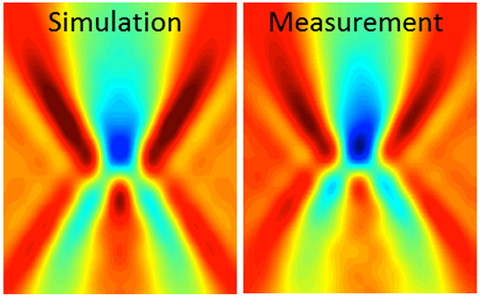
Figure 1. The excellent agreement of measured and simulated TSOM images allow for more reliable quantitative results
Important physical and chemical properties of nanometer scale devices and structures depend on their shape and size. The benefits of nano are already increasing many applications, and are expected to grow significantly. For these applications, measurement accuracy is a fundamental measurement science issue because 1 nm is close to or even below the spatial resolution limit of existing nondestructive measuring instruments. As the nation's leading measurement institute, extending length measurement science and traceability to nanotechnology is part of NIST's mission. Our publications about measuring methods are heavily referenced, and the methods find their way into industry metrology tools and international measurement comparisons. Our measurement methods, reference artifacts and modeling software are used by companies that make metrology tools for nanotechnology applications.
Major Accomplishments
2016
- Implemented the “Full Penn Algorithm” (FPA) for simulating secondary electron generation—not only mean free paths but also energy and angular scattering distributions--in our Monte Carlo simulator. The FPA represents a large correction for low energy electrons and free-electron like materials.
- Applied electron/sample interaction modeling to resolve a long-standing mystery of why there appeared to be an offset between widths of the same feature measured with secondary electrons vs. backscattered electrons.
- Developed 3D nanometescale reconstruction solution useful for essentially all 3D measurements in the SEM.
2015
- Published an invited paper on applications of 3D Monte Carlo SEM modeling to photomask measurements, showing how photomasks charge and reach steady state during the measurement.
- Paper on imaging of buried carbon nanotube in epoxy matrix selected for Nanotechnology cover
- Novel droplet volume calibration method developed. Application of the method to a digital droplet polymerase chain reaction droplet volume measurement supports a DNA concentration SRM being produced by the Biomolecular Sciences Division at NIST. A first draft of the Special Test Method #11050S that describes the specific approach used to obtain the average droplet volume is in preparation and the Report of Measurement with the requisite traceability and uncertainty estimates is ready for on-time delivery.
2014
- Published a paper titled "10 nm Three-Dimensional CD-SEM Metrology" Proc. SPIE 9050 (2014) 90500A by Vladár, et al. and won the Diana Nyyssonen Award for Metrology Best Paper of 2014 SPIE Advanced Lithography
- Measured with world-class accuracy and uncertainty two certified reference materials (CRMs) that have been issued by European cooperators and is now used worldwide.
- Completed 3D SEM model-based measurements on in a collaboration with Intel. Demonstrated sub-nanometer agreement among the results of model-based SEM, transmission electron microscope (TEM), and critical dimension small angle x-ray scattering (CD-SAXS).
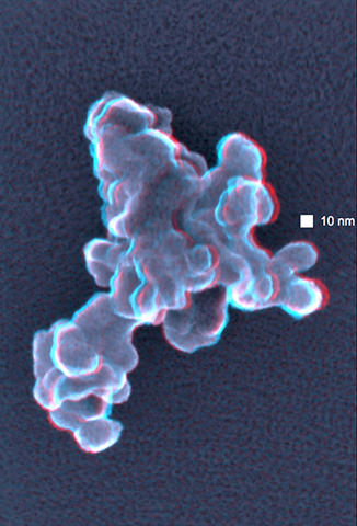
- Development of 3D SEM metrology methods suitable for nanoparticles and nanostructures
- A brain cancer therapy is showing promising results in Phase II clinical trials. The concept is based on a targeted liposome-based nanoparticle delivery system developed by researchers at Georgetown University and SynerGene Therapeutics, Potomac, MD. A recently published journal article presents a comprehensive report on the physical and biological characterization of this increasingly significant approach to cancer treatment. SDMD researchers have played a role in this effort by providing critical dimensional and molecular self-assembly information about the formation of the bimolecular constituents into a complex with an established drug content and stability profile. Since the nanoparticle carries a thoroughly studied regulatory gene, p53, and has been shown to interact with a number of different sensitizing agents, there is reasonable expectation to believe that protocols for the treatment of other cancers may build upon this work.
- Achieved excellent agreement of through-focus scanning optical microscopy (TSOM) simulation and measurement results, which allows for higher confidence in the results and for improved measurement uncertainty
2013
- Keynote presentation titled "Can we get 3D CD Metrology Right?" on 3D metrology of integrated circuits at SPIE Advanced Microlithography
- Successful cooperation with Intel Santa Clara on the application of HIM for lithography photomask repair
- Established a better analysis method of the results of dynamic light scattering (DLS) measurements, which allows for closer agreement among different nanoparticle measurement methods
- Developed and published a new high-performance noise reduction method based on high-speed interferometer-based pixel sorting suitable for SEM and helium ion microscope (HIM) imaging
- Successfully completed a Calibration Services contract for certification of silica nanoparticle reference materials. The studies were conducted by the European Union's Institute for Reference Materials and Measurements (IRMM), Belgium, and included SEM and DLS measurement under accredited International Organization for Standardization (ISO) Quality and Traceability requirements.
Additional Technical Details
Technical Goals:
We carry out the mission of NIST, PML, and EPD by putting state of the art physics to work for nanometer-scale dimensional metrology.
