
Official websites use .gov
A .gov website belongs to an official government organization in the United States.
Secure .gov websites use HTTPS
A lock (
) or https:// means you’ve safely connected to the .gov website. Share sensitive information only on official, secure websites.
Summary
This project focuses on the development of integrated photonics for quantum sensing and information and nonlinear science applications. We combine advanced nanofabrication techniques at the wafer scale and ultralow loss materials, such as tantalum pentoxide and silicon nitride. Compatibility of our advanced device designs and processing techniques at NIST with large-scale semiconductor foundries makes the research widely available. Our team demonstrates robustly designable, high efficiency, and scalable integrated photonics devices that are commercialized for generation of microresonator frequency combs (microcombs), modelocked laser supercontinuum devices, and passive laser beam control and emission across the visible and near-infrared spectral ranges.
Description
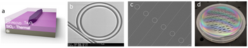
This project develops integrated photonics– devices based on waveguides that are fabricated in a nanoscale device layer on a silicon wafer –for the purposes of exploring nonlinear science, enabling new applications with scalable integrated photonics light sources, and enhancing classical and quantum applications with photonic integrated circuitry. Our research is focused on ultralow loss (~dB per meter) integrated photonics devices in which long storage times for light enables nonlinear conversion and complex photonic circuits. Here at NIST, we have unique capabilities to fabricate such devices at the 100 mm wafer scale with tantalum pentoxide (Ta2O5, tantala) and silicon nitride (Si3N4, SiN) as the device layer material. Tantala is a superior material for integrated photonics due to low residual stress in the device layer, wide transparency window to below 400 nm, and high nonlinear coefficient. SiN is also an exceptional material that supports extremely low loss in the 1550 nm telecom band. We process integrated photonics at the wafer scale with these materials in the NIST Boulder microfabrication facility, utilizing a complete line for semiconductor processing with electron beam and stepper lithography, reactive ion etching, cladding creation by chemical vapor deposition or atomic layer deposition, metals deposition for electrodes and resistive heaters, and wafer separation with optical lithography. The figure below presents our device fabrication capabilities from waveguide structures to wafer scale processing.
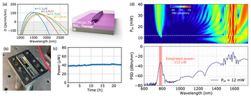
A critical application of integrated photonics is supercontinuum generation with an input modelocked-laser pulse source. We experimentally demonstrate efficient and broadband supercontinuum generation in nonlinear tantala waveguides by use of a 1560 nm femtosecond seed laser. With incident pulse energies as low as 100 pJ, we create spectra spanning up to 1.6 octaves across the visible and infrared. Fabricated devices feature propagation losses as low as 10 dB/m, and they can be dispersion engineered through lithographic patterning for specific applications. We show a waveguide design suitable for low-power self-referencing of a fiber frequency comb that produces dispersive-wave radiation directly at the second harmonic wavelength of the seed laser. A fiber-connectorized, hermetically sealed module with 2 dB per facet insertion loss and watt-level average power handling is also described. Highly efficient and fully packaged tantala waveguides may open new possibilities for the integration of nonlinear nanophotonics into systems for precision timing, quantum science, biological imaging, and remote sensing.
Publications
[1] D. R. Carlson, D. D. Hickstein, W. Zhang, A. J. Metcalf, F. Quinlan, S. A. Diddams, and S. B. Papp, Ultrafast Electro-Optic Light with Subcycle Control, Science 361, 1358 (2018).
[2] D. R. Carlson et al., Photonic-Chip Supercontinuum with Tailored Spectra for Counting Optical Frequencies, Phys. Rev. Applied 8, 014027 (2017).
[3] D. R. Carlson et al., Self-Referenced Frequency Combs Using High-Efficiency Silicon-Nitride Waveguides, Opt. Lett., OL 42, 2314 (2017).
[4] K. F. Lamee, K. F. Lamee, D. R. Carlson, D. R. Carlson, Z. L. Newman, Z. L. Newman, S.-P. Yu, S.-P. Yu, S. B. Papp, and S. B. Papp, Nanophotonic Tantala Waveguides for Supercontinuum Generation Pumped at 1560 Nm, Opt. Lett., OL 45, 4192 (2020).
[5] D. D. Hickstein, D. R. Carlson, H. Mundoor, J. B. Khurgin, K. Srinivasan, D. Westly, A. Kowligy, I. I. Smalyukh, S. A. Diddams, and S. B. Papp, Self-Organized Nonlinear Gratings for Ultrafast Nanophotonics, Nature Photonics 13, 7 (2019).
[6] D. R. Carlson, P. Hutchison, P. Hutchison, D. D. Hickstein, S. B. Papp, and S. B. Papp, Generating Few-Cycle Pulses with Integrated Nonlinear Photonics, Opt. Express 27, 37374 (2019).
[7] D. R. Carlson, D. R. Carlson, D. D. Hickstein, S. B. Papp, and S. B. Papp, Broadband, Electro-Optic, Dual-Comb Spectrometer for Linear and Nonlinear Measurements, Opt. Express, OE 28, 29148 (2020).
[8] E. Baumann et al., Dual-Comb Spectroscopy with Tailored Spectral Broadening in Si3N4 Nanophotonics, Opt. Express, OE 27, 11869 (2019).
Major Accomplishments
- Development of ultralow power, packaged modules for frequency comb self-referencing.
- Exploration of novel nonlinear phenomena with integrated photonics, including self-organized gratings, high-harmonic generation, nonlinear spectroscopy, and dual comb spectroscopy.
- Collaboration with astronomical observatories for exoplanet spectroscopy with integrated photonics supercontinuum generators.