
Official websites use .gov
A .gov website belongs to an official government organization in the United States.
Secure .gov websites use HTTPS
A lock (
) or https:// means you’ve safely connected to the .gov website. Share sensitive information only on official, secure websites.
Optoelectrical Characterization of Nanostructured Photovoltaic Materials and Devices
Summary
Photovoltaics technology is usually categorized into three generations: 1) devices based on polysilicon; 2) devices based on thin-film direct bandgap semiconductors; and 3) devices that exploit nanoscale three-dimensional (3D) structures to achieve higher efficiencies at affordable manufacturing cost. Regardless of category, in the absence of regulatory subsidies, large-scale implementation of photovoltaic (PV) devices will require efficiencies exceeding 15 %, lifetimes of ten years with minimal degradation in performance, and power-to-cost ratios roughly comparable to carbon-based fuels. At present, although promising candidates are appearing, no technology in any of the three generations fully meets these requirements. The goal of this project is to develop measurement tools and techniques to characterize the physical processes related to light absorption, energy transfer and carrier dynamics in the third generation of PV materials and devices.
Description
In a typical PV cell, light absorption creates excitons that separate into charge carriers under the influence of the electric field of a p-n junction. The free carriers must leave the PV device, reaching and crossing their respective contacts, to generate useful power. Usually, only part of the solar spectrum is absorbed. Additionally, the photon absorption length is larger than that of defect-mediated recombination events, which yields a device thickness based on an unsatisfactory design trade-off between light collection and carrier extraction.
Third generation nanostructured PV devices offer the opportunity to independently engineer photon absorption, free carrier generation, and pathways for carrier extraction. Light capture can be enhanced by nanoscale couplers such as plasmonic antennas and antireflection coatings. The absorption spectrum may also be engineered by exploiting a broad range of nanomaterials, such as quantum dots and organic molecules forming p- and n-, or donor and acceptor, heterojunction interfaces that permeate the material. Excitons are separated into free electrons and holes at these bulk heterojunction interfaces. The extraction of electrons and holes into contacts also requires good connectivity and transport properties in the both p- and n- regions. At present, the development of third generation PV devices lags far behind alternate PV technologies in both efficiency and cost. Here, nanoscale metrology must focus on characterizing morphology, probing transport properties, and measuring interfacial electronic behavior. However, measurements in these materials are complicated by the range of relevant length scales, with exciton diffusion occurring over a few tens of nanometers, but photon absorption occurring over micrometers.
With such a variety and complexity of processes and length scales affecting real-world devices built of different materials, microscopic insight into device operation cannot be delivered by a single measurement setup. Capitalizing on diverse expertise at the CNST in scanning probe techniques, nanofabrication, nanophotonics and electrical measurements, we are building a suite of tools capable of analyzing the critical physical processes at the relevant length scales.
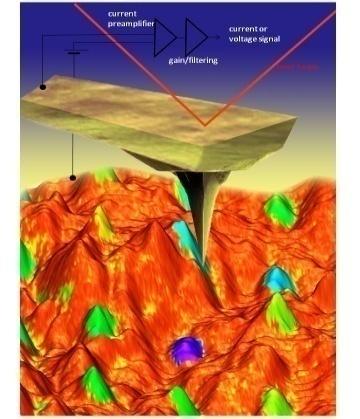
The first dedicated tool already in operation is based on a modified scanning probe instrument capable of operating in high vacuum or in a controlled gas environment. We study the photocurrent generation at the nanoscale in order to understand the correlation between the local structure and the collection efficiency in organic PV material based on a blend of electron-donating polymer, poly (3 - hexylthiophene), with small-molecule acceptor, phenyl C61 butyric acid methyl ester (PCBM). In optimally performing devices, donor and acceptor materials are expected to form interpenetrating networks mixed at the lengths below 50 nm; however the material mixing and separation in real devices is poorly known. In the first approach, we fabricate fixed nanoscale contacts by evaporating metals through stencil masks made within silicon nitride membranes. The contacts can be made smaller or larger than the characteristic lengths of the material mixing or of the exciton diffusion length, enabling the meaningful analysis of the inhomogeneous PV materials. The metal contacts are interrogated using a conducting Atomic Force Microscope (AFM) as a miniature probe station. Alternatively, we probe the photocurrent generation directly by AFM tip with various conductive coatings. In order to access the material properties throughout device in all three dimensions, we develop sectioning techniques optimized for the material being studied. In the case of organic PVs, we use shallow angle microtomy to create wedge-shaped devices and to enable the measurement of the interior of the film with scanning probes. The data are used to build effective models relating the nanoscale properties to the macroscopic device performance.
Other tools under development include nanoscale vibrational microscopy and tip-enhanced Raman microscopy for obtaining structural and chemical information on local composition.
Selected Publications
- Imaging of nanoscale charge transport in bulk heterojunction solar cells, B. H. Hamadani, N. Gergel-Hackett, P. M. Haney, and N. B. Zhitenev, Journal of Applied Physics 109, 124501 (2011).
NIST Publication Database Journal Web Site
- Three dimensionally structured interdigitated back contact thin film heterojunction solar cells, C. M. Hangarter, B. H. Hamadani, J. E. Guyer, H. Xu, R. Need, and D. Josell, Journal of Applied Physics 109, 073514 (2011).
NIST Publication Database Journal Web Site
- Origin of nanoscale variations in photoresponse of an organic solar cell, B. H. Hamadani, S. Jung, P. M. Haney, L. J. Richter, and N. B. Zhitenev, Nano Letters 10, 1611-1617 (2010).
NIST Publication Database Journal Web Site