Summary
Our goal is to develop and demonstrate a MEMS-based methodology for evaluating time-dependent mechanical properties of materials that undergo exposure to extreme and harsh environments (e.g., temperature extremes, high radiation, corrosive chemistries, etc.). Such test methods hold promise for providing a high throughput route to thoroughly measuring the remaining lifetime of highly irradiated materials present in today's nuclear power plants, as well as the suitability of new alloys for next generation nuclear plants.
Description
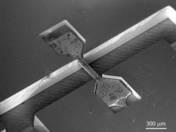
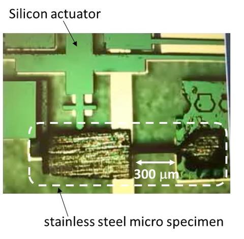
A stainless steel micro tensile specimen in a silicon frame.
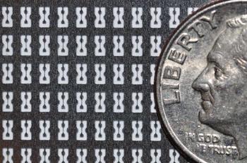
Classically, measurement of the mechanical properties and reliability of bulk-scale materials is performed with macroscopic specimens and methods. Specimen preparation limitations, miniaturized load-frame tooling problems, and inadequate understanding of the roles of specimen size and constraint on properties have hindered the use of micrometer-scale specimens and techniques. We are developing a new approach that combines specimen preparation techniques such as focused ion beam (FIB) milling with microtechnology-based test tools. This will enable evaluation of large populations of specimens, on-chip, and in parallel, to provide statistically significant results. Properties of small-scale structures are linked to those of bulk-scale structures through application of three-dimensional, imaged-based finite element modeling. Currently, we use FIB to obtain micrometer-scale specimens from structural materials irradiated in test reactors, accelerators, or working power reactors for insertion into prefabricated on-chip test structures. Ultimately, we will fabricate arrays of test structures with on-chip control, actuation, and sensing. This will provide long-term, in situ testing of time-dependent mechanical properties of materials to be used in NGNP and fusion reactors.
Major Accomplishments
MEMS-based fatigue test instrument and fatigue testing of micro aluminum specimens
We leveraged MEMS technology to develop a silicon micromachined fatigue load frame which includes an on-chip actuator and displacement sensor. The device is operated under an optical microscope, and performs bending fatigue tests on micro sized metal specimens inserted into it. The specimens have gauge widths of about 100 μm and gauge thickness of about 25 μm. Fatigue failure is detected by the on-chip sensor, and specimen strains are obtained via digital image correlation. The specimens themselves are made separately. The chips can be re-used after specimens have fractured.
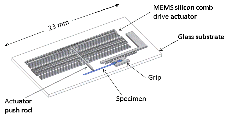
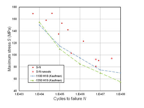
We demonstrated this technique by generating an S-N curve for Al 1145 H19 micro specimens, and measuring the bending stiffness of stainless steel micro specimens. In particular, since generating an S-N curve requires testing of many specimens and with each test being time consuming, a potential advantage of this MEMS approach is low-cost batch fabrication of the silicon devices and the potential to run many chips/specimens in parallel, which would enable highly efficient generation of large data sets. Another advantage is the small size of the actuator which could allow in-situ fatigue testing in harsh environments.
Publications:
L.A. Liew, D.T. Read, N. Barbosa III, “MEMS-based universal fatigue test technique,” Experimental Mechanics, Vol 53(5), pp. 783-794, 2013.
Micro tensile testing on stainless steel micro specimens
We used silicon micromachining techniques to fabricate frames into which micro stainless steel tensile specimens are placed. The silicon frame consists of a stationary outer structure connected by tethers to a movable central platform. Grips consist of etched recesses with the same geometry as the specimen’s ends. One end of the specimen is gripped in the stationary structure and the other end is gripped in the movable platform. The silicon chip is then placed under an optical microscope, and the movable platform is pulled by a custom external actuator to apply tensile loads to the specimen. Force is measured with a load cell and strains are obtained via digital image correlation.

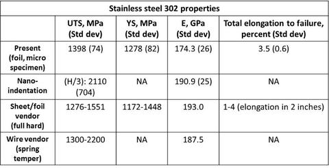
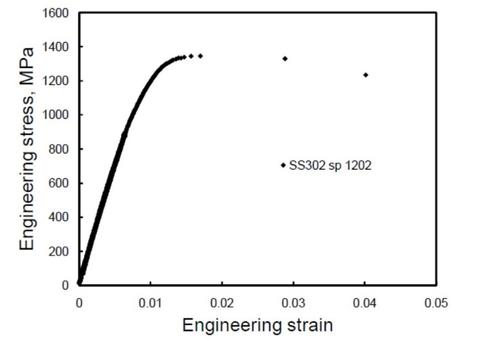
We obtained engineering stress-strain curves of stainless steel 302 micro specimens with gauge section dimensions of 360 μm long x 70 μm wide x 25 μm thick. The specimens were fabricated separately, by a commercial vendor, from stainless steel foils. The properties obtained from our micro tensile tests are in agreement with those specified by the material vendor, and with properties we measured using nanoindentation. This technique allows for tensile testing of extremely small volumes of material – smaller than the state of the art for bulk materials testing – and would be advantageous for testing of in-service traditional structural materials and materials that have been subjected to harsh environments.
Publications:
D.T. Read and N. Barbosa III, “Coming full circle: the application of microtechnology techniques to evaluate bulk materials,” Proc. 2010 MRS Fall Meeting, Vol 1298, 2011.
Keywords
structural materials, mechanical testing, MEMS, microsystems, materials characterization, energy, infrastructure, electronics, manufacturing, microscale
Associated Product(s)
Project Summary (PDF)

