Summary
Our goal is to develop, advance, and demonstrate measurements that facilitate Nanoimprint Lithography (NIL) as a viable technology for the patterning of robust, reliable, and functional nanostructures with dimensions smaller than 25 nm. These measurements will be critical as NIL transitions from a novel laboratory patterning technique to a commercial nanomanufacturing method for applications as diverse as semiconductors, patterned data storage media, high brightness light emitting diodes (LEDs), and other emerging forms of nanotechnology.
Description
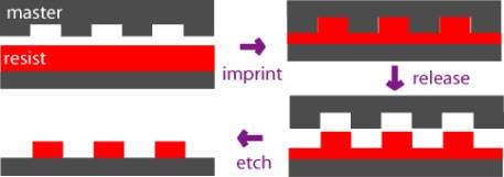
Nanoimprint Lithography (NIL) was originally perceived as a versatile, low-cost, and high-resolution patterning alternative for optical lithography in CMOS fabrication. However, it is becoming apparent that NIL has great potential for nanotechnology in general. It is capable of patterning sub-10 nm features directly into a range of materials, even functional materials, and not just sacrificial resist formulations. Intense R&D activities are currently centered on CMOS logic devices, bit patterned data storage media, high brightness LEDs, patterned biological devices, and optical devices. Our approach is to develop measurement platforms that quantify the quality of the pattern or feature that has been fabricated by NIL. These quantitative assessments of the imprint process are necessary inputs to optimize the NIL based R&D processes and move from the novel demonstrations or devices in the lab to the high volume nanomanufacturing required for commercialization. To accomplish this we leverage our internal expertise in accurately measuring physical shape and properties at the nanoscale. The way that the NIL process itself influence both the shape and properties of the imprinted materials has a profound impact on the performance, robustness and quality of the imprinted device. By providing the measurement component of the processing-properties-structure paradigm, we can accelerate the development of products based on the NIL technology.
Major Accomplishments
- The target for NIL patterning is expanding from semiconductors devices to a range of technologies where nanoscale patterning has yet to be realized, including data storage media, high brightness LEDs, displays, sensors, and lab on a chip devices.
- NIST has emerged, in the face of diverging interests within the NIL community, as leaders in the materials and metrology needs for this rapidly expanding technology. We lead panel discussions and present numerous plenary/invited lectures on this topic at major conferences.
- NIST measurements of the residual stresses in the NIL process provide seminal insight for developing roll-to-roll imprint processes, spawning worldwide interest by several other research groups.
- First demonstration of the direct patterning of functional, ultralow-k dielectric insulator materials. Our measurements quantify the fidelity of the pattern transfer process and the unique way in which the NIL processes affect the porosity characteristics critical to the application.
Additional Technical Details
Pattern Shape Metrology: Recently we developed a pattern shape metrology based on specular X-ray reflectivity (SXR). We found that the reflectivity off a patterned surface (mold or imprint) could be fit to extract the scattering length density profile as a function of height. If the pitch or width of the pattern is known, the density profile can be converted into an absolute pattern cross-section. The key to this technique is the effective medium approximation (EMA) where the density of the lines and spaces in the pattern are laterally averaged together. This occurs when the coherence length of the X-ray beam is larger than the pattern. Here we determined the limits of this method by quantifying the coherence length of our slit shaped X-ray beam. The coherence length was highly anisotropic. In the direction parallel to the slit axis the coherence length is on the order of 900 nm, but over 25 µm in the orthogonal in plane direction. These anisotropic length scales establish critical limits in terms of the size and orientation of the pattern shapes that can be quantified using our SXR method. More fundamentally, our systematic studies of the imprinted patterns with varying periodicity have also revealed a way to quantify the coherence length of an X-ray source. In the past this has been a difficult parameter to quantify.
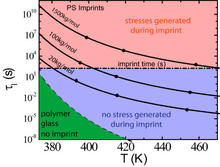
Imprint Induced Stresses: The thermal embossing form of NIL relies upon the pressure induced flow of a viscous polymer melt into the mold cavities. Given the nanoscale dimensions of these cavities, the shear stresses generated during this flow can be significant. This can lead to large levels of residual stress in the imprinted pattern. Our measurements show that these residual stresses can be controlled by understanding the rheology of mold fill. At a given imprint temperature, there is a characteristic relaxation time for the polymer melt defined by the terminal time τ for viscoelastic flow. If the duration of the imprinting process is longer than τ, then the shear induced stresses have time to relax and the pattern is stress free. If τ is longer than the imprint, then residual stress are frozen into the pattern. Our analysis shows that these stresses can be minimized by reducing the molecular mass of the polymer, increasing the imprint temperature, or imprinting for longer times. These measurements are of direct relevance to roll-to-roll imprint processes where the mold is separated from imprint at elevated temperatures.
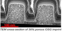
Porous Imprint Materials: One advantage of NIL is that it can directly pattern functional materials, beyond resists for pattern transfer. An example of recent interest is the direct patterning of porous ultra low-k materials for semiconductor interconnects. This has the potential to significantly reduce the fabrication cost for semiconductors, by eliminating costly lithography and pattern transfer steps. However, the way that the imprinting process affects critical pore characteristics is then of relevance. We have developed measurements that fully characterize the critical properties of a highly porous organosilicate glasses (OSGs) directly patterned by NIL. SXR pattern shape metrology is used to not only to precisely evaluate the fidelity of the pattern transfer process, but also quantify shrinkage when the imprinted patterns are vitrified into a hard ceramic at high temperature. We have also adapted X-ray porosimetry, positron annihilation lifetime spectroscopy, and cross-sectional transmission electron microscopy measurements to fully quantify how the imprinting process changes the porosity characteristics.
Associated Product(s)
Project Summary (PDF)


