
Official websites use .gov
A .gov website belongs to an official government organization in the United States.
Secure .gov websites use HTTPS
A lock (
) or https:// means you’ve safely connected to the .gov website. Share sensitive information only on official, secure websites.
Summary
Develop and apply advanced measurement methods, electric field reference materials, and COMSOL models to make electrical scanning probe microscopes (eSPMs), such as the scanning Kelvin force microscope (SKFM) and the scanning microwave microscope (SMM), more quantitative and accurate for measuring variations in the electrical properties of complexly structured future nanodevices and materials.
Description
Electric Field Gradient reference prototype
Electrical scanning probe microscopes (eSPMs) are a subset of scanning probe microscopes which measure some electrical parameter as well as surface topography. These include techniques such as scanning capacitance microscopy (SCM), scanning spreading resistance microscopy (SSRM), conductive atomic force microscopy (C-AFM), scanning Kelvin force microscopy (SKFM), and scanning microwave impedance microscopy (SMIM). These techniques can provide a high spatial resolution mapping of an electrical property across a material or within an electronic device. For example, SCM has been used to measure the local tip-to-sample differential capacitance of cross-sectioned transistors, which is then related to the local sample dopant density of the semiconductor. When applied to a source/drain region, the two-dimensional dopant profile of the active region of the device can be obtained with spatial resolution of 10 nm. Quantitative interpretation of eSPM images requires some level of modeling of the physics of the tip-sample interaction. The most accurate results require consideration of the details of the tip shape, the measurement conditions, and the physics of the tip-sample interaction.
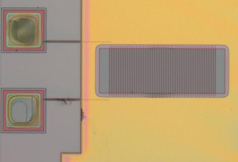
Reference Materials – We are building and characterizing test chips containing prototype Electric Field Gradient Reference Materials and Tip Profiler Artefacts. SKFM is often calibrated by measuring the contact potential between the tip and a freshly deposited gold film. For our reference materials (Figure 1), the dimensions and applied potentials of the devices are known precisely, allowing the actual electric field at the surface to be calculated precisely. This will allow a known staircase in surface potential to be produced, producing a long-term stable artefact to calibrate both the accuracy and spatial resolution of a probe based electric field measurement. Such artefacts have never been produced before. The major difficulty is producing an easily useable structure, validating model results, and producing a validated calibration procedure. Other structures on the test chip include buried interdigitated electrodes and field plates surrounded by a ground electrode. These structures are proving useful to help understand how tip shape effects measured potential across an abrupt boundary and as a means of isolating samples from the effects of surrounding material.
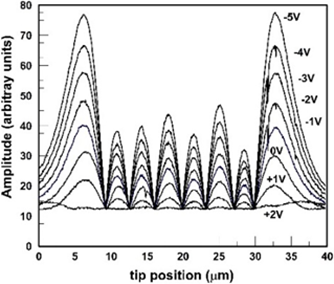
Subsurface Imaging – We are investigating multiple techniques for subsurface imaging with eSPMs. We have imaged floating and grounded buried lines beneath as much as 3 micrometers of oxide using SMM [1]. We have imaged biased metal lines at similar depths with electrostatic force microscopy (EFM), Figure 2. We have developed a variation of EFM, which we have dubbed remote bias induced electrostatic force microscopy (RB-EFM), where instead of inducing tip vibration with an ac bias applied to the tip, we apply the ac bias to the remote electrodes. When applied to structures with multiple buried electrodes we have found that we can improve both the spatial resolution and depth sensitivity by biasing adjacent electrodes 180o out of phase with each other. In Figure 3, RB-EFM line scans of a set of interdigitated electrodes, buried beneath 1200 nm of oxide are shown. Each set of interdigitated lines is biased 180o out of phase with their opposing interdigitated lines. Lines were biased at a series of discrete dc voltages (-5 V to +2 V). The measured signal is proportional to the amplitude of cantilever vibration. The signal is forced to a minimum at the mid-point between adjacent lines by the change in phase in the driving signal between adjacent lines. As the dc bias on the lines is increased from -5 V to +2 V, the amplitude steadily decreases. Because the adjacent lines act as active electrical shield for any central line, a signal can be detected from lines buried quite deeply. We estimate RB-EFM can detect buried metal lines up to 20 micrometers deep, suggesting applications to back end of the line metallization fault detection.
Modeling – Accurate quantitative interpretation of SMM, SCM, SKFM images is intrinsically tied to the quality of modelling available. The COMSOL software has proven to be capable of three-dimensional modeling of eSPMs and considerable improvement is possible, though this will require validation against well specified measurements. The overarching goal here is to produce a “Virtual eSPM” in COMSOL merging the electrostatic, micro-mechanical and semiconductor physics modules with models of real tips and samples. Such a capability would, for example, allow simplified extraction of dopant profiles from differential capacitance images, potential distributions from electric field images, or current distributions from magnetic field images. It would also be a powerful platform to understand the effects of additional physics not usually considering in SPM such as surface states on capacitance or surface layer oxidation on work function. Once a base model is in place, the addition of more esoteric physics can be considered.
Current Thrusts – SPMs are ideally suited for rapid evaluation of candidate two-dimensional materials for spintronic and quantum applications, high-band gap, photovoltaic and electro-optic materials; and for determining the spatial variation of electrical properties within nanostructured devices. We are pursuing multiple applications and seek additional collaborations in these areas.
Major Accomplishments
2019
Fabricated first proto-type electric filed gradient test structure. Demonstrated remote bias induced electrostatic force microscopy (RB-EFM).