
Official websites use .gov
A .gov website belongs to an official government organization in the United States.
Secure .gov websites use HTTPS
A lock (
) or https:// means you’ve safely connected to the .gov website. Share sensitive information only on official, secure websites.
Dimensional Metrology for Nanoscale Patterns
Summary
| Our goal is to develop and demonstrate precise measurement methods that quantify the physical shape, critical dimensions (CD) and the structure of nanoscale patterns and thin films using scattering and reflectivity methods based on X-rays and neutrons. We will work with consortia and leaders within the semiconductor industry to establish these methods on systems of immediate technical interest, in ways that both complements and extends their current metrology tools. |

|
Description
|
|
Major Accomplishments
- NIST measurements of line width roughness by CD-SAXS were quantitatively benchmarked against state-of-the-art CD-SEM in a round robin including the SEMATECH Advanced Metrology Group and Intel
- CRADA signed with Intel to develop quantitative CD-SAXS line width and line edge roughness measurements
- This includes custom pattern fabrication by Intel and one of their assignees (KW Choi) working full time at NIST
- Industrial Technology Research Institute (ITRI, Taiwan) announces the launch of a CD-SAXS research program in 2009. Staff exchange program established with NIST and ITRI to facilitate technology transfer
- CD-SAXS achieves the first example of 3D metrology for interconnects
- Preliminary measurements on FINFET structures demonstrate the feasibility on these buried structures. Such measurements are not possible with current methods
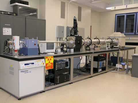
- Lab scale prototype instrument built for feasibility studies on NIST campus
Additional Technical Details

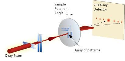
Line width roughness (LWR): The International Technology Roadmap for Semiconductors (2007 update) states that one of the greatest metrology challenges facing the industry is the quantification of line width roughness (LWR), defined as the variation in line width relative to the average value. Even today, at the 65 nm technology node, the existing methods lack the required resolution. We have been developing CD-SAXS methods that quantify both the amplitude and frequency of LWR with very high accuracy. To demonstrate these methods, test patterns with controlled LWR were collaboratively designed and fabricated by Intel, NIST, and Sematech. The inset of the figure above shows an image of one of these test patterns while the main portion of the figure shows the resulting scattering pattern. The analysis to quantify the roughness parameters has been recently published and is listed among our selected publications. Attempts to compare the CD-SAXS and CD-SEM LWR values proved problematic, because the electron beam of the SEM destroyed the resist pattern. A second study of lines with controlled roughness that were transferred into inorganic hard mask materials is near completion and will allow a quantitative comparison between the two techniques.

CD-SAXS versus CD-SEM: CD-SEM is the industry standard measurement tool for quantifying the physical dimensions of nanoscale patterns. Any new metrology must first be benchmarked against CD- SEM. To accomplish this, a series of line- space grating patterns with periodicities of 150 nm, 200 nm and 250 nm and variable line width was quantified by both techniques. The CD-SAXS parameters were obtained by fitting the line shapes with a trapezoidal cross section while the CD-SEM analysis focused on top-down images of the lines. The comparison of the line widths in the figure below shows excellent agreement between the two methods. The linear fit through the data has a slope of 1.03 and an offset of just 0.2 nm. However, this excellent agreement only exists when comparing the CD-SEM line widths to the bottom (or maximum) width of the trapezoid. If the average CD- SAXS trapezoid width is used the slope and offset deviate by as much as 0.94 and 13.03 nm, respectively. This indicates that CD-SEM is biased toward the bottom width of the feature in top down image.

Laboratory Scale CD-SAXS: CD-SAXS is a transmission scattering technique. High energy X-rays that can penetrate the supporting Si substrate are required. Such X-rays can be obtained at a synchrotron source where the X-ray energies are tunable. Also, the synchrotron X-ray beam has a flux that is 4 to 5 orders of magnitude larger than that from a lab instrument. However, coupling CD-SAXS to a synchrotron facility limits its utility to industry as a CD metrology. We have built a lab scale CD- SAXS prototype using a rotating anode Mo X-ray tube (high energy) source. Despite the limited flux, this instrument is capable of collecting high quality data. Line space gratings are being measured both at the APS synchrotron and in-house. As shown below excellent agreement exists between the line width from the two instruments. This year we have made arrangements to connect our CD-SAXS camera to a developmental compact laboratory scale X-ray synchrotron source as a potential route for the development of CD-SAXS as a viable industrial measurement tool.