Official websites use .gov
A .gov website belongs to an official government organization in the United States.
Secure .gov websites use HTTPS
A lock (
) or https:// means you’ve safely connected to the .gov website. Share sensitive information only on official, secure websites.
2000 and later - History of NIST Quantum Voltage Standards
2005
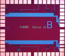
NIST integrated an advanced programmable standard chip into a new soldered, flex-bonded package, which is more reliable than the earlier spring fingerboard design. This chip also offers twice the maximum voltage, 2.6 volts, of the original programmable standards because the junctions are double-stacked for the first time. The new design with niobium electrodes and molybdenum-disilicide barriers can be stacked and patterned with dry-etch processing. The area of each junction is 4 micrometers by 8 micrometers, and there are 67,410 junctions on the 1-centimeter-square chip. By redesigning the circuit to optimize it for three voltage levels, a 100-fold improvement in voltage resolution was achieved. This chip was used in the NIST Gaithersburg voltage laboratory in the "watt balance" experiment for redefining the kilogram from 2004 until 2010, when it was damaged by a lightning strike to the building.
(Artifact 9, Citation: Y. Chong et al., IEEE Trans. Inst. Meas., vol. 54, pp. 616-619, April 2005)
2007
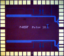
In a step toward highly accurate ac quantum voltage standards, a NIST pulse-driven chip generated accurate 0.1-volt waveforms, the first waveforms above 100 millivolts—the threshold for practical measurements. The chip used junctions made of niobium electrodes with molybdenum-disilicide barriers, each 8 micrometers by 4 micrometers in size. This circuit was the first to be used in the voltage calibration laboratory at NIST Gaithersburg to make the first ac-to-dc voltage calibrations.
(Artifact 12, Citation: S. P. Benz et al, "An AC Josephson Voltage Standard for AC-DC Transfer Standard Measurements," IEEE Trans. Inst. Meas., vol. 56, pp. 239-243, April 2007)
2008
NIST developed the "quantum watt," the world's first quantum-based ac power standard, which reduced measurement uncertainty for calibrations of power and energy meters. These meters measure the electric power grid, determining how much power customers use. The quantum watt improves capabilities to quantify the power grid and will help make the "smart grid" work. A programmable Josephson voltage standard operating as an accurate low-frequency ac reference was integrated into the power standard. The system features greatly improved traceability of electrical power to the quantum-based international units for the volt and ohm.
2009
NIST demonstrated the first chip to produce quantum-based accurate ac voltage waveforms above 275 millivolts. This record voltage showed that a 1-volt circuit potentially could be produced with only eight arrays, although such a design has yet to be demonstrated. The chip has two arrays, each with 6,400 junctions that have double-stacked niobium electrodes and niobium-silicide barriers. Each junction is 14 micrometers by 3.5 micrometers in size.
(Artifact 13, Citation: S. P. Benz et al, "Progress toward a 1 V pulse-driven ac Josephson voltage standard," IEEE Trans. Inst. Meas., vol. 58, no. 4, pp. 838-843, April 2009.)
2011
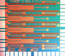
NIST begins producing and delivering 10-volt programmable standards with about 300,000 triple-stacked junctions, capable of both ac and dc voltage. This is the first programmable voltage standard with triple-stacked junctions to produce stable quantized steps above 10 volts with practical 1 milli-ampere current operating margins. A key advance is the use of niobium junctions with niobium-silicide barriers that produce stable steps and have uniform electrical properties. The chip is 12 millimeters by 17 millimeters in size.
(Artifact 10, Citation: P.D. Dresselhaus et al, "10 Volt Programmable Josephson voltage standard circuits using NbSi-barrier junctions," to appear in IEEE Trans. Appl. Supercond., June 2011)
2011
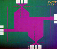
NIST researchers and collaborators used a quantum-voltage-based "Johnson noise" thermometer (JNT) to make the first practical electronic measurement of the Boltzmann constant, a fundamental constant that is important for measuring temperature. The electronics are calibrated with noise-like signals synthesized by a superconducting voltage source. The chip has a novel design and uses only two arrays of four junctions each to generate the low voltages needed for the experiment.
The junctions have niobium electrodes and niobium-silicide barriers and are 14 micrometers by 7 micrometers in size. The idea of using pulse-driven Josephson junction arrays to synthesize waveforms for this new approach to JNT was conceived by John Martinis of NIST in 2000 and first demonstrated in 2005. The JNT technique is simpler and more compact than gas-thermometry methods for measuring the Boltzmann constant and could advance international efforts to revamp the world's scientific measurement system.
(Artifact 14, Citation: S.P. Benz, A. Pollarolo, J. Qu, H. Rogalla, C. Urano, W.L. Tew, P.D. Dresselhaus and D.R. White. 2011. An electronic measurement of the Boltzmann Constant. Metrologia. March 30.)