
Official websites use .gov
A .gov website belongs to an official government organization in the United States.
Secure .gov websites use HTTPS
A lock (
) or https:// means you’ve safely connected to the .gov website. Share sensitive information only on official, secure websites.
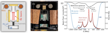
Chip-Scale Atomic Beam System
Published Patent Application Number: 18/832,716
Problem
Current atomic beam systems (such as Cs beam tubes for atomic clock) exist either in lab-scale vacuum systems or in custom vacuum tubes.
Invention
The invention is a device for creating a collimated atomic beam in an evacuated vacuum package fabricated from lithographically defined or machined, planar structures and with components to source atomic vapor and passive pumps to maintain vacuum conditions. We have developed a chip-scale system for producing an atomic beam.
Potential Commercial Applications
Applications include chip-scale atomic clocks and interferometers. Chip scale clocks are primarily used in cell phone base stations and underwater oil and gas exploration.
Competitive Advantage
This invention provides a lithographically fabricated process to realize atomic beams with high collimation in a more manufacturable and compact package. Our value added is to reach better long-term instability than vapor cell chip-scale systems in a smaller package than conventional Cs beam systems.