
Official websites use .gov
A .gov website belongs to an official government organization in the United States.
Secure .gov websites use HTTPS
A lock (
) or https:// means you’ve safely connected to the .gov website. Share sensitive information only on official, secure websites.
Resistivity and Hall Measurements
Sample Geometry | Definitions for Resistivity Measurements | Resistivity Measurements | Resistivity Calculations | Definitions for Hall Measurements | Hall Measurements | Hall Calculations
The following procedures for carrying out Hall measurements provide a guideline for the beginning user who wants to learn operational procedures, as well as a reference for experienced operators who wish to invent and engineer improvements in the equipment and methodology.
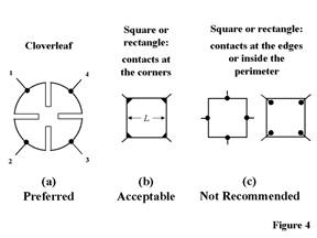
It is preferable to fabricate samples from thin plates of the semiconductor material and to adopt a suitable geometry, as illustrated in Fig. 4. The average diameters (D) of the contacts, and sample thickness (d) must be much smaller than the distance between the contacts (L). Relative errors caused by non-zero values of D are of the order of D/L.
The following equipment is required:
- Permanent magnet, or an electromagnet (500 to 5000 gauss)
- Constant-current source with currents ranging from 10 µA to 100 mA (for semi-insulating GaAs, ρ ≈ 107 Ω·cm, a range as low as 1 nA is needed)
- High input impedance voltmeter covering 1 µV to 1 V
- Sample temperature-measuring probe (resolution of 0.1 °C for high accuracy work)
Definitions for Resistivity Measurements
Four leads are connected to the four ohmic contacts on the sample. These are labeled 1, 2, 3, and 4 counterclockwise as shown in Fig. 4a. It is important to use the same batch of wire for all four leads in order to minimize thermoelectric effects. Similarly, all four ohmic contacts should consist of the same material.
We define the following parameters (see Fig. 2):
ρ = sample resistivity (in Ω·cm)
d = conducting layer thickness (in cm)
I12 = positive dc current I injected into contact 1 and taken out of contact 2. Likewise for I23, I34, I41, I21, I14, I43, I32 (in amperes, A)
V12 = dc voltage measured between contacts 1 and 2 (V1 - V2) without applied magnetic field (B = 0). Likewise for V23, V34, V41, V21, V14, V43, V32 (in volts, V)
The data must be checked for internal consistency, for ohmic contact quality, and for sample uniformity.
- Set up a dc current I such that when applied to the sample the power dissipation does not exceed 5 mW (preferably 1 mW). This limit can be specified before the automatic measurement sequence is started by measuring the resistance R between any two opposing leads (1 to 3 or 2 to 4) and setting
I < (200R)-0.5.
(6)
- Apply the current I21 and measure voltage V34
- Reverse the polarity of the current (I12) and measure V43
- Repeat for the remaining six values (V41, V14, V12, V21, V23, V32)
Eight measurements of voltage yield the following eight values of resistance, all of which must be positive:
R21,34 = V34/I21, R12,43 = V43/I12,
R32,41 = V41/I32, R23,14 = V14/I23,
R43,12 = V12/I43, R34,21 = V21/I34,
R14,23 = V23/I14, R41,32 = V32/I41.
(7)
Note that with this switching arrangement the voltmeter is reading only positive voltages, so the meter must be carefully zeroed.
Because the second half of this sequence of measurements is redundant, it permits important consistency checks on measurement repeatability, ohmic contact quality, and sample uniformity.
- Measurement consistency following current reversal requires that:
R21,34 = R12,43
R32,41 = R23,14
R43,12 = R34,21
R14,23 = R41,32
(8)
- The reciprocity theorem requires that:
R21,34 + R12,43 = R43,12 + R34,21 and
R32,41 + R23,14 = R14,23 + R41,32.
(9)
If any of the above fail to be true within 5 % (preferably 3 %), investigate the sources of error.
- The sheet resistance RS can be determined from the two characteristic resistances
RA = (R21,34 + R12,43 + R43,12 + R34,21)/4 and
RB = (R32,41 + R23,14 + R14,23 + R41,32)/4
(10)
via the van der Pauw equation [Eq. (3)]. For numerical solution of Eq. (3), see the routine in Section IV. If the conducting layer thickness d is known, the bulk resistivity ρ = RSd can be calculated from RS.
Definitions for Hall Measurements
The Hall measurement, carried out in the presence of a magnetic field, yields the sheet carrier density ns and the bulk carrier density n or p (for n-type or p-type material) if the conducting layer thickness of the sample is known. The Hall voltage for thick, heavily doped samples can be quite small (of the order of microvolts).
The difficulty in obtaining accurate results is not merely the small magnitude of the Hall voltage since good quality digital voltmeters on the market today are quite adequate. The more severe problem comes from the large offset voltage caused by nonsymmetric contact placement, sample shape, and sometimes nonuniform temperature.
The most common way to control this problem is to acquire two sets of Hall measurements, one for positive and one for negative magnetic field direction. The relevant definitions are as follows (Fig. 3):
I13 = dc current injected into lead 1 and taken out of lead 3. Likewise for I31, I42, and I24.
B = constant and uniform magnetic field intensity (to within 3 %) applied parallel to the z-axis within a few degrees (Fig .3). B is positive when pointing in the positive z direction, and negative when pointing in the negative z direction.
V24P = Hall voltage measured between leads 2 and 4 with magnetic field positive for I13. Likewise for V42P, V13P, and V31P.
Similar definitions for V24N, V42N, V13N, and V31N apply when the magnetic field B is reversed.
The procedure for the Hall measurement is:
- Apply a positive magnetic field B
- Apply a current I13 to leads 1 and 3 and measure V24P
- Apply a current I31 to leads 3 and 1 and measure V42P
- Likewise, measure V13P and V31P with I42 and I24, respectively
- Reverse the magnetic field (negative B)
- Likewise, measure V24N, V42N, V13N, and V31N with I13, I31, I42, and I24, respectively
The above eight measurements of Hall voltages V24P, V42P, V13P, V31P, V24N, V42N, V13N, and V31N determine the sample type (n or p) and the sheet carrier density ns. The Hall mobility can be determined from the sheet density ns and the sheet resistance RS obtained in the resistivity measurement. See Eq. (2).
This sequence of measurements is redundant in that for a uniform sample the average Hall voltage from each of the two diagonal sets of contacts should be the same.
Steps for the calculation of carrier density and Hall mobility are:
- Calculate the following (be careful to maintain the signs of measured voltages to correct for the offset voltage):
VC = V24P - V24N, VD = V42P - V42N,
VE = V13P - V13N, and VF = V31P - V31N.
(11)
- The sample type is determined from the polarity of the voltage sum VC + VD + VE + VF. If this sum is positive (negative), the sample is p-type (n-type).
- The sheet carrier density (in units of cm-2) is calculated from
ps = 8 x 10⁻⁸IB/[q(VC + VD + VE + VF)]
if the voltage sum is positive, or
ns = |8 x 10⁻⁸ IB/[q(VC + VD + VE + VF)]|
if the voltage sum is negative,
(12)
where B is the magnetic field in gauss (G) and I is the dc current in amperes (A).
- The bulk carrier density (in units of cm-3) can be determined as follows if the conducting layer thickness d of the sample is known:
n = ns/d
p = ps/d
(13)
- The Hall mobility µ = 1/qnsRS (in units of cm2V-1s-1) is calculated from the sheet carrier density ns (or ps) and the sheet resistance RS. See Eq. (2).
The procedure for this sample is now complete. The final printout might contain (Sample Hall Worksheet):
- Sample identification, such as ingot number, wafer number, sample geometry, sample temperature, thickness, data, and operator
- Values of sample current I and magnetic field B
- Calculated value of sheet resistance RS, and resistivity ρ if thickness d is known
- Calculated value of sheet carrier density ns or ps, and the bulk-carrier density n or p if d is known
- Calculated value of Hall mobility µ
Notice of Online Archive: This page is no longer being updated and remains online for informational and historical purposes only.
Contacts
-
PML webmaster